The ability to control machines by thought is a long-time dream of people; especially for those who are paralyzed. In recent years, technological progress has accelerated the progress of the human brain machine interface (BMI). For biomedical applications, researchers at Duke University have successfully used neural probes to develop signal processing ASICs and electronic circuit systems for wireless transmission of power and information. The next step is to develop component packaging technology. However, how will these components connect to each other?
Size and reliability are the two most important elements for biomedical implants. Two packaging technologies in the microelectronics industry (flip chip bonding and flexible PCB carrier) are just right for this application.Flip chip bonding technology has been developed for more than 30 years. The advantages of this technology are small size, high wiring density, and improved electrical properties due to short pins4. Another advantage of flip-chip bonding technology is that multiple chips of different sizes can be packaged on the same PCB carrier to form a multi-chip module. This type of packaging can eliminate large and unreliable connectors.
In addition, the flexible PCB carrier board made of polyimide can be bent and folded, which can make full use of space to make small-sized components. However, because polyimide materials are only suitable for low-temperature joining technology (the process temperature is less than 200 degrees Celsius), it is necessary to use thermosetting adhesive instead of solder to provide mechanical and electrical connection. In this study, we use low-cost pillar gold bumping technology instead of tin-lead bumping technology used in other similar applications.
In order to develop a manufacturing process suitable for biomedical applications, we design and manufacture test chips using polyimide as the substrate. These test chips are used to verify the manufacturing process after being stamped with pillar-shaped gold bumps. We tested the conductive and insulating thermally hardened adhesives respectively, and after doing the temperature cycle test, the contact resistance was measured to evaluate the reliability of the product.
Joining technology
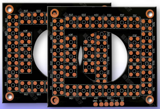
We hope to use pillar gold bump technology and thermally hardened adhesive to develop a reliable process to bond the diced chip to the flexible PCB carrier. In this study, we tested two bonding methods; the first method uses insulating thermosetting adhesive, and the second method uses conductive adhesive and insulating underfill. Each test component is composed of a test circuit PCB carrier board and a dummy chip. The PCB carrier board of the pin array package is also designed on the same polyimide PCB carrier board, so that it can be used to test the nerve signal amplifier chip in the future.
Preparation of the simulation chip: In order to make the soft simulation chip as hard as the silicon chip, we have to add a reinforcing member on the back of the soft simulation chip. However, the reinforcing member provided by the PCB carrier manufacturer is too soft, so we replaced the reinforcing member provided by the manufacturer with a small 1mm thick microscope slide. Cylindrical gold bumps: The simulation chip and the chip’s cylindrical gold bumps used in the test are all made with a manual gold ball bonding machine (Kulicke & Soffa’s 4524AD).
Insulated thermosetting adhesive bonding: In the insulating thermosetting adhesive bonding method, the chip with long columnar gold bumps and the PCB carrier board are bonded with insulating thermosetting adhesive. The alignment and bonding of the chip and the PCB carrier board are performed by a flip chip bonding machine (SUSS Microtec's FC150). The steps of joining are as follows:
1. Load the chip with long pillar-shaped gold bumps and the PCB carrier board into the flip chip bonder.
2. The chip and the PCB carrier board are aligned by a flip chip bonder.
3. Coat the insulating thermosetting adhesive on the PCB carrier board.
4. Connect the chip to the PCB carrier board according to the conditions in Table 2 and Figure 3.
5. The adhesive is thermally hardened under the pressure of joining, and then cooled down before the pressure is released.
Joining technology of conductive adhesive
In the conductive adhesive bonding method, a chip with long pillar-shaped gold bumps is first placed in a thin layer of silver glue. Then connect the chip with silver glue to the PCB carrier board with insulating thermosetting glue. The alignment and bonding of the chip and the PCB carrier also use a flip chip bonding machine. The joining steps are as follows:
1. Load the chip with long pillar-shaped gold bumps into the flip chip bonder.
2. Place the glass slide on the suction cup on the PCB carrier.
3. Coat a thin layer of conductive silver glue on the glass slide. Note: Dilute the conductive silver glue by 10% to achieve a better adhesion effect.
4. Use a flip chip bonder to spread the conductive silver paste to a thickness of 30 microns.
5. Press the chip with the pillar-shaped gold bumps into the 30-micron-thick conductive silver glue layer.
6. Remove the glass slide and put it on the PCB carrier board.
7. Coat insulating heat-curing adhesive on the PCB carrier board.
8. Align the chip with the PCB carrier board, and then bond it with the PCB carrier board through glue.
9. The adhesive is thermally hardened under the pressure of joining, and then cooled down before the pressure is released.

Temperature cycle test: Temperature cycle test is often used to verify the reliability of the joint. During the temperature cycle test, the temperature and the resistance between a pair of bumps on the simulated chip are recorded every 30 seconds.
The temperature change conditions of the temperature cycle test are set as follows:
1. Keep it at 85 degrees Celsius for 10 minutes.
2. Cool down to minus 10 degrees Celsius as quickly as possible.
3. Keep it at minus 10 degrees Celsius for 10 minutes.
4. Increase the temperature to 85 degrees Celsius as quickly as possible.
5. Repeat this temperature change cycle.
The simulation chip is cut from the polyimide substrate, and the glass slide is bonded to enhance the structural strength of the flexible simulation chip, and pillar-shaped gold bumps are placed, and then the two methods mentioned above (insulating thermosetting adhesive bonding technology), Conductive thermal hardening adhesive bonding technology) to join the simulation chip and the flexible PCB carrier board. Since this simulation chip made on the polyimide substrate is translucent, we can visually inspect the bonding interface. The cylindrical gold bumps appear to be compressed evenly, which means that the flatness is well controlled. The accuracy of the alignment is controlled within 3 microns. It can be seen that there are some air bubbles in the adhesive layer, but these air bubbles do not seem to affect the performance.
There are several advantages to the joining technique using pillar-shaped gold bumps and glue. First of all, this method is suitable for diced chips. In fact, using a soft emulation chip as a test component is a relatively inexpensive and practical way to develop bonding technology. The translucent test components are even more beneficial than expected when using polyimide as the substrate. Since the test component is semi-transparent, we can easily use optical micromirrors to check the quality of the joint. Using insulated thermosetting adhesive bonding technology, the process steps are relatively simple, and there is no need for cleaning steps and additional underfill. There are several steps in the bonding method of conductive adhesive that need to be carefully controlled, especially the application of silver glue and dipping glue. In addition, for the consideration of mechanical strength, it is necessary to add an underfilling step. The common disadvantage of these two methods is that the curing time (10 minutes) of the adhesive is too long; as far as research is concerned, this is acceptable.
However, for mass production, a glue with a shorter curing time is necessary. We believe that when the adhesive and underfill are cured, they can tighten the chip and PCB carrier, thus enhancing the quality of the joint. In the temperature cycle test, the average resistance of the insulated thermosetting adhesive bonding technology was in line with our expectations; this result was also comparable to the results of other units. Using insulated thermosetting adhesive bonding technology, the components prepared by flip-chip bonding on the flexible PCB substrate and the commercially produced ceramic pin array package components have the same electrical performance. In addition, this technology has the advantages of small size and adaptability to different shapes.
In order to bond the ASICS chip of the neural signal amplifier to the flexible PCB carrier board by flip-chip packaging, we developed and evaluated two bonding methods, and used the simulation chip manufactured on the polyimide substrate for the development and testing of the manufacturing process. Based on the consideration of simple manufacturing process and good reliability, we use insulated thermosetting adhesive bonding technology and pillar gold bump technology. We also use this method to connect the ASICS chip of the neural signal amplifier to the pin array package PCB carrier board. The first trial produced a 100% functional product.