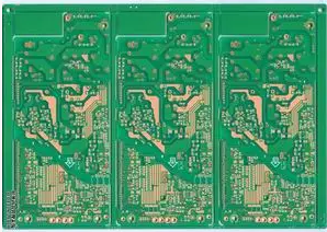
Conductive hole Via hole is also known as via hole. In order to meet customer requirements, the circuit board via hole must be plugged. After a lot of practice, the traditional aluminum sheet plugging process is changed, and the circuit board surface solder mask and plugging are completed with white mesh. hole. Stable production and reliable quality. Via hole plays the role of interconnection and conduction of circuits. The development of the electronic industry also promotes the development of PCB circuit boards, and also puts forward higher requirements on the production process and surface mount technology of the printed circuit board. Via hole plugging technology came into being, and should meet the following requirements at the same time:

(1) There is copper in the via hole, and the solder mask can be plugged or not plugged;
(2) There must be tin and lead in the via hole, with a certain thickness requirement (4 microns), and no solder mask ink should enter the hole, resulting in tin beads hidden in the hole;
(3) The through holes must have solder mask ink plug holes, opaque, and must not have tin rings, tin beads, and flatness requirements.
With the development of electronic products in the direction of "light, thin, short, and small", PCBs have also developed to high density and high difficulty. Therefore, a large number of SMT and BGA PCBs have appeared, and customers require plugging when mounting components, mainly including Five functions:
(1) Prevent the tin from passing through the component surface through the via hole to cause a short circuit when the PCB is wave soldered; especially when we put the via on the BGA pad, we must first make the plug hole and then gold-plated to facilitate the BGA soldering.
(2) Avoid flux residue in the via hole;
(3) After the surface mounting of the electronics factory and the assembly of the components are completed, the PCB must be vacuumed to form a negative pressure on the testing machine to complete:
(4) Prevent surface solder paste from flowing into the hole, causing false soldering and affecting placement;
(5) Prevent the tin beads from popping up during wave soldering, causing short circuits.
Realization of Conductive Hole Plugging Process
For surface mount boards, especially the mounting of BGA and IC, the via hole plug must be flat, convex and concave plus or minus 1mil, and there must be no red tin on the edge of the via hole; the via hole hides the tin ball, in order to reach the customer According to the requirements, the via hole plugging process can be described as diverse, the process flow is particularly long, the process control is difficult, and the oil is often dropped during the hot air leveling and the green oil solder resistance test; the oil explosion after curing and other problems occur. Now according to the actual conditions of production, the various plugging processes of PCB are summarized, and some comparisons and explanations are made in the process and advantages and disadvantages:
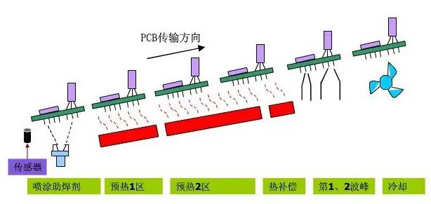
Note: The working principle of hot air leveling is to use hot air to remove excess solder from the surface and holes of the printed circuit board, and the remaining solder is evenly coated on the pads, non-resistive solder lines and surface packaging points, which is the surface treatment method of the printed circuit board one.
1. Hole plugging process after hot air leveling
The process flow is: board surface solder mask-HAL-plug hole-curing. The non-plugging process is adopted for production. After the hot air is leveled, the aluminum sheet screen or the ink blocking screen is used to complete the via hole plugging required by the customer for all the fortresses. The plug hole ink can be photosensitive ink or thermosetting ink. In the case of ensuring the same color of the wet film, the plug hole ink is best to use the same ink as the board surface. This process can ensure that the through holes will not lose oil after the hot air is leveled, but it is easy to cause the plugging ink to contaminate the board surface and uneven. Customers are prone to false soldering (especially in BGA) during mounting. So many customers do not accept this method.
2. Hot air leveling and plug hole technology
2.1 Use aluminum sheet to plug the hole, solidify, and polish the board to transfer the graphics
This technological process uses a numerical control drilling machine to drill out the aluminum sheet that needs to be plugged to make a screen, and plug the holes to ensure that the via hole plugging is full. The plug hole ink can also be used with thermosetting ink. Its characteristics must be high in hardness., The shrinkage of the resin is small, and the bonding force with the hole wall is good. The process flow is: pre-treatment - plug hole - grinding plate - pattern transfer - etching - board surface solder mask
This method can ensure that the plug hole of the via hole is flat, and there will be no quality problems such as oil explosion and oil drop on the edge of the hole when leveling with hot air. However, this process requires one-time thickening of copper to make the copper thickness of the hole wall meet the customer's standard. Therefore, the requirements for copper plating on the entire plate are very high, and the performance of the plate grinding machine is also very high, to ensure that the resin on the copper surface is completely removed, and the copper surface is clean and not contaminated. Many PCB factories do not have a one-time thickening copper process, and the performance of the equipment does not meet the requirements, resulting in not much use of this process in PCB factories.
2.2 After plugging the hole with aluminum sheet, directly screen-print the board surface solder mask
This process uses a CNC drilling machine to drill out the aluminum sheet that needs to be plugged to make a screen, install it on the screen printing machine to plug the hole, and park it for no more than 30 minutes after completing the plugging, and use 36T screen to directly screen the surface of the board. The process flow is: pre-treatment-plug hole-silk screen-pre-baking-exposure-development-curing
This process can ensure that the via hole is well covered with oil, the plug hole is flat, and the color of the wet film is consistent. After the hot air is leveled, it can ensure that the via hole is not tinned and the tin bead is not hidden in the hole, but it is easy to cause the ink in the hole after curing. The soldering pads cause poor solderability; after the hot air is leveled, the edges of the vias are blistered and oil is removed. It is difficult to control the production by this process method, and the process engineers must use special processes and parameters to ensure the quality of the plug holes.
2.3 The aluminum sheet is plugged into the hole, developed, pre-cured, and polished, and then solder resist is performed on the surface of the board.
Use a CNC drilling machine to drill out the aluminum sheet that requires plugging holes to make a screen, install it on the shift screen printing machine for plugging holes. The plugging holes must be full and protruding on both sides. The process flow is: pre-treatment-plug hole-pre-baking-development-pre-curing-board surface solder mask
Because this process uses plug hole curing to ensure that the via hole does not lose oil or explode after HAL, but after HAL, it is difficult to completely solve the problem of tin bead storage in the via hole and tin on the via hole, so many customers do not accept it.
2.4 The board surface solder mask and plug hole are completed at the same time.
This method uses a 36T (43T) screen, installed on the screen printing machine, using a pad or a bed of nails, and when completing the board surface, all the vias are plugged. The process flow is: pretreatment-screen printing- -Pre-baking--Exposure--Development--Curing
The process time is short and the equipment utilization rate is high. It can ensure that the via holes will not lose oil after the hot air leveling, and the via holes will not be tinned. However, due to the use of silk screen for plugging the holes, there is a large amount of air in the via holes., The air expands and breaks through the solder mask, resulting in cavities and unevenness. There will be a small amount of through holes hidden in the hot air leveling. At present, after a large number of experiments, our company has selected different types of inks and viscosity, adjusted the pressure of the screen printing, etc., and basically solved the voids and unevenness of the vias, and has adopted this process for mass production.