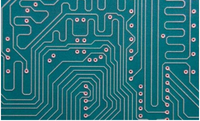
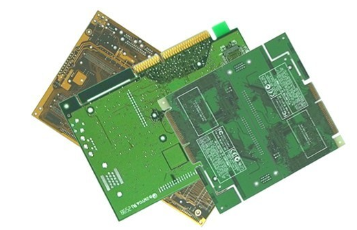
Over the years, engineers have developed several methods to deal with the noise that causes high-speed digital signal distortion in PCB circuit board design. As design technology advances with the times, our technical complexity to deal with these new challenges is also increasing. At present, the speed of digital design systems is measured in GHz, and the challenges caused by this speed are far greater than in the past. Since the edge rate is measured in picoseconds, any impedance discontinuity, inductance or capacitance interference will adversely affect the signal quality. Although there are various sources that can cause signal interference, a special and often overlooked source is vias.

Hidden dangers in simple vias
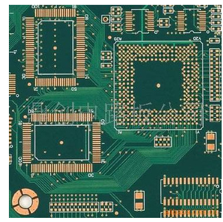
High-density interconnection(HDI), high-level count printed circuit boards, and thick backplane/middle board via-hole signals will be affected by more jitter, attenuation, and higher bit error rate(BER), resulting in data being corrupted at the receiving end. Misinterpretation.
Take the backplane and daughter card as examples. When encountering impedance discontinuities, the focus is on the connectors between these boards and the mother card. Normally, these connectors are very matched in terms of impedance, and the discontinuity actually originates from the via.
As the data rate increases, the amount of distortion caused by the plated through hole (PTH) via structure also increases-usually at an exponential rate that is much higher than the relevant data rate increment. For example, the distortion of a PTH via at 6.25Gb/s is usually more than twice the distortion produced at 3.125Gb/s.
The presence of unwanted via stub extension layers on the bottom and top layers makes the vias show lower impedance discontinuities. One way for engineers to overcome the extra capacitance of these vias is to minimize their length, thereby reducing their impedance. This is the origin of back drilling.
Use back drilling technology
By removing the via remnants, back drilling has been widely regarded as a simple and effective method to minimize the signal attenuation of the channel. This technique is called fixed-depth drilling, and it uses traditional numerical control (NC) drilling equipment. At the same time, the technology can be applied to any type of circuit board, not just a thick board like a backplane.
Compared with the original via, the drill bit used in the back drilling method has a slightly larger diameter in order to remove unnecessary conductor stubs. The drill bit is usually 8mil larger than the main drill, but many manufacturers can meet the more stringent specifications.
It should be remembered that the distance between the trace and the plane needs to be large enough to ensure that the back-drilling procedure will not penetrate nearby traces and planes. To avoid penetrating traces and planes, the recommended spacing is 10mil.
Generally speaking, there are many benefits to reducing the length of via stubs through back drilling, including:
Decrease the deterministic jitter by orders of magnitude, resulting in a lower bit error rate.
Reduce signal attenuation through improved impedance matching.
Reduce the electromagnetic interference / electromagnetic compatibility radiation from the stub, and increase the channel bandwidth.
Reduce resonance excitation mode and crosstalk between vias.
With lower manufacturing costs than sequential lamination, the design and layout influence is minimized.
Communicate design intent through back drilling
With the frequent use of back-drilling technology in high-density interconnection and high-speed design applications, this method also brings reliability issues. Some of the problems include the lack of design guidelines, manufacturing tolerances, and how to ensure that the design intent is well communicated to the manufacturing unit.
So, how do you ensure that your manufacturer has all the information needed for back-drilled target vias and plated through-hole components? How to keep track of multiple levels of back-drilled specifications throughout the design process?
In fact, what is needed is very simple: a simple visual configuration tool integrated into the design rules, allowing you to specify different back drill configurations for the selected object. Then, you can let the software that knows which vias need back-drilling to help you do the work.