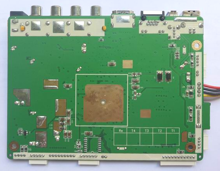
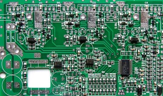
Solder mask (also known as solder mask) is a layer of specially designed pattern care film formed on the surface of PCB in PCB manufacturer. It is formed by screen printing or covering solder mask ink, and then through a series of processing. PCB solder mask can avoid short circuit caused by tin on non soldering parts during welding process, save solder, avoid electric short circuit caused by moisture and chemical erosion between conductors, and avoid electric open circuit caused by scratch and scratch caused by various human factors in the process of PCB production, welding and transportation, resist the annihilation and corrosion of PCB by various despicable background, and ensure the development of printed circuit board Normal function, but also can satisfy the customer different color, the appearance need. Because the solder mask of PCB has many advantages, the mask solder mask is almost always selected in PCB preset and fabrication.
Because the dielectric constant of the air is 1.0005, and the dielectric constant and damage factor of the existing common solder mask ink are about 3.9 and 0.03, because this is similar to the exposed outer circuit, and the transmission background of the line after covering the solder mask has changed greatly, which will cause the electrical performance of the outer circuit to be changed.

The influence of solder mask layer on the electrical properties of external circuit is mainly introduced by pate PCB
Reduce the impedance value of the outer circuit: the special property impedance of the signal line, when the line is covered with solder mask ink, the capacitance C value increases, so the impedance value of the line will be reduced;
Increase the damage loss of outer circuit transmission: in the process of signal transmission, the damage will be revealed, mainly including conductor damage and medium loss, where the medium loss is directly proportional to the medium layer damage factor (medium damage, Tanδ C is the damage factor, K is a constant). When it is considered appropriate to cover with solder mask ink, the damage factor of ink is large, so it will increase Damage and loss of transmission line;
Reduce the transmission speed of the outer circuit: because the transmission speed of the signal line depends on the speed of light and the dielectric constant of the medium layer (where K1 is the constant, C is the speed of light, and ε is the dielectric constant of the medium, DK), and the dielectric constant of the solder mask is longer than that of the air, because the transmission speed of the signal line will be reduced after covering the solder mask ink Degree.
For high speed PCB, the existence of solder mask has many advantages, such as anti welding, protective board, insulation, good-looking, but also has a great impact on the initiation of outer signal transmission. Because of this, it is of great significance to understand the influence of the existing solder resist ink on the impedance and damage of the external circuit for the PCB manufacturer's circuit preset and PCB impedance control.