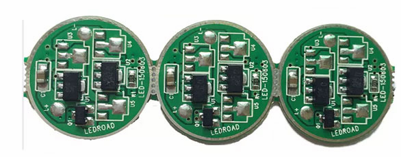
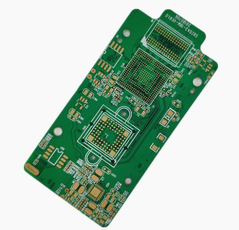
PCB circuit board surface treatment process
After the customer's technology draws the PCB circuit board, it will be sent to the PCB proofing factory or mass production. When we place the order to the circuit board factory, we will attach a PCB circuit board processing process description document, one of which is to Indicate which PCB surface treatment process to choose, and different PCB surface treatment processes will have a greater impact on the final PCB processing quotation, and different PCB surface treatment processes will have different charges. The editor would like to talk to you about the current common PCB surface treatment processes, the advantages and disadvantages of different PCB surface treatment processes and applicable scenarios in many domestic PCB board factories.
Then why do we need to perform special treatment on the PCB surface?
Because copper is easily oxidized in the air, the copper oxide layer has a great influence on welding, and it is easy to form false welding and virtual welding. In severe cases, the pads and components cannot be welded. For this reason, PCBs are in production. At this time, there will be a process to coat (plating) a layer of material on the surface of the pad to protect the pad from oxidation.
At present, the PCB surface treatment processes of domestic circuit board factories include: spray tin (HASL, hotairsolderleveling), tin, immersion silver, OSP (anti-oxidation), chemical immersion gold (ENIG), electroplating gold, etc., of course, special There are also some special PCB circuit board surface treatment processes in the application.

Comparing different PCB surface treatment processes, their costs are different. Of course, the occasions used are also different. Only the right ones are not selected. There is no perfect PCB surface treatment process. The price can satisfy all PCB application scenarios), so there are so many crafts for us to choose. Of course, each craft has its own merits, and the existence of them is reasonable. The key is that we must know them and use them well.
Let's compare the advantages and disadvantages and applicable scenarios of different PCB circuit board surface treatment processes.
Advantages: low cost, smooth surface, good weldability (in the absence of oxidation).
Disadvantages: It is easy to be affected by acid and humidity and cannot be stored for a long time. It must be used up within 2 hours after unpacking, because copper is easily oxidized when exposed to the air; it cannot be used for double-sided boards because the second side after the first reflow soldering It's already oxidized. If there are test points, solder paste must be printed to prevent oxidation, otherwise it will not be in good contact with the probes.
spray tin plate (HASL, HotAirSolderLevelling, hot air levelling)
Advantages: lower price, good welding performance.
Disadvantages: Not suitable for welding pins with fine gaps and components that are too small, because the surface flatness of the spray tin plate is poor. Solder beads are prone to be produced during circuit board processing, and it is easier to cause short circuits for fine pitch components. When used in the double-sided SMT process, because the second side has undergone a high-temperature reflow soldering, it is very easy to spray tin and re-melt, resulting in tin beads or similar droplets that are affected by gravity into spherical tin dots, which make the surface even worse. Flattening affects welding problems.
The tin spraying process used to dominate the circuit board surface treatment process. In the 1980s, more than three-quarters of the circuit boards used the spray tin process, but the industry has been reducing the use of the tin spray process in the past ten years. It is estimated that about 25%-40% of the PCBs use the spray tin process. Craft. The tin spray process is dirty, unpleasant, and dangerous, so it has never been a favorite process, but the tin spray process is an excellent process for larger components and wires with larger spacing. In high-density PCBs, the flatness of the tin spraying process will affect subsequent assembly; therefore, HDI boards generally do not use the circuit board tin spraying process. With the advancement of technology, the industry now has a tin spraying process suitable for assembling QFPs and BGAs with smaller pitches, but there are fewer practical applications. At present, some circuit board factories use OSP technology and immersion gold technology to replace the tin spraying process; technological developments have also caused some circuit board factories to adopt tin and silver immersion processes. Coupled with the lead-free trend in recent years, the use of tin spraying technology has been further restricted. Although there has been so-called lead-free tin spraying, this may involve equipment compatibility issues.
OSP (OrganicSolderingPreservative, anti-oxidation)
Advantages: It has all the advantages of PCB bare copper welding. The expired (three months) board can also be resurfaced, but usually only once.
Disadvantages: easily affected by acid and humidity. When used in the secondary reflow soldering, it needs to be completed within a certain period of time, and usually the effect of the second reflow soldering will be relatively poor. If the storage time exceeds three months, it must be resurfaced. It must be used up within 24 hours after opening the package. OSP is an insulating layer, so the test point must be printed with solder paste to remove the original OSP layer before it can contact the pin point for electrical testing.
It is estimated that about 25%-30% of PCBs currently use OSP process, and the proportion has been rising (it is likely that OSP process has now surpassed tin spraying and ranks first). The OSP process can be used on low-tech PCBs as well as high-tech PCBs, such as PCBs for single-sided TVs and boards for high-density chip packaging. For BGA, OSP has more applications. If PCB does not have functional requirements for surface connection or limitation of storage period, OSP process will be the most ideal surface treatment process.
Immersion Gold (ENIG, ElectrolessNickelImmersionGold)
Advantages: It is not easy to oxidize, can be stored for a long time, and the surface is flat, suitable for welding fine-gap pins and components with small solder joints. The first choice for PCB boards with buttons (such as mobile phone boards). Reflow soldering can be repeated many times without reducing its solderability. It can be used as a substrate for COB (ChipOnBoard) wire bonding.
Disadvantages: high cost, poor welding strength, because the electroless nickel plating process is used, it is easy to have the problem of black disk. The nickel layer will oxidize over time, and long-term reliability is a problem.
Immersion gold process is different from OSP process. It is mainly used on boards with functional connection requirements and a long storage period on the surface, such as the keypad area of a mobile phone, the edge connection area of the router housing, and the electrical contacts for the elastic connection of the chip processor. Area. Due to the flatness problem of the tin spraying process and the removal of the flux of the OSP process, the use of immersion gold was widely used in the 1990s; later due to the appearance of black disks and brittle nickel-phosphorus alloys, the application of immersion gold was reduced., But at present almost every high-tech PCB factory has sinking gold wire. Considering that the solder joint will become brittle when removing the copper-tin intermetallic compound, there will be many problems in the relatively brittle nickel-tin intermetallic compound. Therefore, portable electronic products (such as mobile phones) almost all use copper-tin intermetallic compound solder joints formed by OSP, immersion silver or immersion tin, and immersion gold is used to form the key area, contact area and EMI shielding area, which is the so-called selective Immersion gold craft. It is estimated that about 10%-20% of PCBs currently use electroless nickel/immersion gold processes.
Immersion Silver (ENIG, ElectrolessNickelImmersionGold)
Immersion Silver is cheaper than Immersion Gold. If the PCB has connection functional requirements and needs to reduce costs, Immersion Silver is a good choice; coupled with Immersion Silver's good flatness and contact, then the Immersion Silver process should be chosen. Immersion Silver has many applications in communication products, automobiles, and computer peripherals, as well as in high-speed signal design. Since Immersion Silver has good electrical properties that other surface treatments cannot match, it can also be used in high-frequency signals. EMS recommends using the immersion silver process because it is easy to assemble and has better checkability. However, due to defects such as tarnishing and solder joint voids, the growth of immersion silver is slow (but not decreasing). It is estimated that about 10%-15% of PCBs currently use immersion silver technology.
Shen Tin (ENIG, ElectrolessNickelImmersionGold)
The introduction of tin sinking into the surface treatment process has occurred in the past ten years, and the emergence of this process is the result of the requirements of production automation. Immersion tin does not bring any new elements into the soldering area, which is especially suitable for backplanes for communication. Tin will lose its solderability beyond the storage period of the board, so tin sinking requires better storage conditions. In addition, the tin-immersion process is restricted due to the carcinogenic substances contained in it. It is estimated that about 5%-10% of PCBs currently use the tin-immersion process.