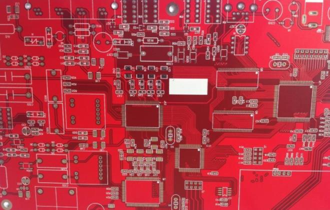
Copper immersion process for PCB production
Perhaps we may be surprised that only two sides of the substrate of the circuit board have copper foil, and the half-waist is the insulating layer, then there is no need for them to conduct between the two sides of the circuit board or between the multi-layer circuit boards? How can the lines on both sides be linked together so that the current can pass smoothly?
Below, please see the circuit board manufacturer for you to analyze this very wonderful process-copper sinking (PTH).
Immersion copper is the abbreviation of Eletcroless Plating Copper, also called plated through hole, abbreviated as PTH, which is a self-catalyzed oxygenation recovery response. After the two or more layers are drilled, the PTH process must be implemented.
The effect of PTH: On the non-conductive hole wall substrate that has been drilled, a thin layer of chemical copper is deposited chemically to serve as the substrate for subsequent copper electroplating.
PTH process decomposition: alkaline degreasing-two or three-stage reverse rinsing-roughening (micro-etching)-two-stage reverse rinsing-pre-soaking-activation-two-stage reverse rinsing-degumming-second-stage reverse rinsing-copper deposition-two Level reverse rinsing - pickling
PTH detailed process explanation:
Alkaline degreasing: remove oil stains, fingerprints, oxygen compounds, and dust on the surface of the board; adjust the pore wall from negative charge to positive charge, which facilitates the adsorption of colloidal palladium in the subsequent process; clean after degreasing Implement according to the guidance requirements, and try to perform inspection and determination with heavy copper backlighting.

2. Micro-etching: remove the oxygen compounds on the board surface, roughen the board surface, and ensure that the subsequent copper immersion layer and the bottom copper of the substrate have a satisfactory bonding force; the new copper has a strong shielding of the face Active, can absorb colloidal palladium beautifully;
3. Pre-soaking: The main purpose is to take care of the palladium tank from the pollution of the pre-treatment tank liquid, and to extend the life of the palladium tank. The main components are exactly the same as the palladium tank except for palladium chloride, which can effectively wet the hole wall. It is easy for the subsequent activation solution to enter the hole as early as possible to perform sufficient effective activation;
4. Activation: After the pre-treatment alkaline degreasing polarity adjustment, the positively charged pore wall can be used to adsorb enough negatively charged colloidal palladium particles to ensure the uniformity, continuity and precision of subsequent copper precipitation; Because this degreasing and activation are critical to the quality of subsequent copper deposits. Control essentials: the prescribed time; the concentration of standard stannous ion and chloride ion liquid; the specific gravity, acidity and temperature are also very important, and they must be strictly controlled in accordance with the operating instructions.
5. Degumming: remove the stannous ions in the food made of flour and water fermented from the colloidal palladium particles, so that the palladium nuclei in the colloidal particles are exposed, and the reaction of chemical copper precipitation is started by directly using catalysis. Experience shows that using fluorine Boric acid is a better choice as an antigelling agent.
6. Copper deposition: After the activation of the palladium nucleus induces the autocatalytic reaction of the electroless copper deposition, the new chemical copper and the reaction by-product hydrogen can be used as the reaction reactant to catalyze the response, so that the copper deposition response is continuously implemented. After this step, a layer of chemical copper can be deposited on the plate surface or the hole wall. During the process, the bath liquid should maintain normal air mixing to convert more soluble divalent copper.
The quality of the copper sinking process is directly related to the quality of the produced circuit boards. It is the main source process of impermissible vias and bad open and short circuits, and it is inconvenient for visual inspection. The subsequent processes can only be screened by destructive experiments. The method implements effective analysis and monitoring of a single PCB board, so the problem must be a batch problem once it appears, even if the test is not completed, the final product causes a great quality hazard and can only be discarded in batches. Therefore, it is necessary to strictly follow the instructions in the operation guide. Variable operations.