Rigid-flex board manufacturing process and manufacturing process of rigid-flex board
1. Medium:
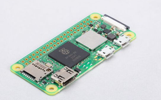
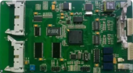
As a special interconnect technology, flex-rigid multilayer printed board can reduce the assembly size and weight of electronic products, prevent wiring problems, and realize three-dimensional assembly under different assembly conditions. The characteristics of thinness, shortness, and smallness have been widely used in computers, avionics and military electronic equipment. However, rigid-flex printed boards also have huge craftsmanship, high construction costs, and are not easy to change and repair. This article mainly discusses the improvement of rigid-flex multilayer printed board lamination, outer layer imaging, etc., and talks about the construction of rigid-flex printed boards.
2. Rigid-flex printed board layout:
The rigid-flex printed board is to bond two (or more) rigid outer layers on the flexible printed board. The circuit on the rigid layer and the circuit on the flexible layer are connected to each other through metallized holes. Each rigid-flex printed board has one or more rigid areas and one or more flexible areas.
1. Rigid-flex printed board materials: In addition to rigid materials (such as epoxy glass cloth laminates and prepregs or polyimide laminates and corresponding prepregs), rigid-flex printed boards also use flexible materials.

1. Flexible material:
2. Copper foil:
The copper foil used for printed boards is mainly divided into electrolytic copper foil (ED) and rolled copper foil (RA). Electrolytic copper foil is formed by an electroplating method. The copper particle crystal condition is vertical needle-like, which is easy to form a vertical line edge during etching, which is beneficial to the construction of dense lines; but when the bending radius is less than 5mm or static bending, the needle Shaped layout is prone to fracture; therefore, the flexible copper clad substrate is mostly used for calendered copper foil, and its copper particles are arranged in a horizontal axis shape, which can adapt to repeated deflection.
2. Imaging and etching of flexible inner layer:
1. Pre-treatment: The copper foil of the copper clad laminate has been treated with anti-oxidation, and the copper foil has a dense oxide protective film. Therefore, the flexible copper clad laminate must be washed and roughened before imaging. However, because the flexible plate is easy to deform and twists, a public pumice grinding plate (Pumice) machine or micro-etching (Micro-etching) can be adopted-the general manufacturer proposes to adopt micro-etching to reduce the extra equipment investment. During the process of micro-etching, the roughening level and average roughness of the board surface should be controlled. It is recommended that the micro-etching solution adopt sodium persulfate (Na2S2O4) and sulfuric acid (H2SO4) type micro-etching solution to avoid excessive roughening of the board surface. Or the board surface of the department is not sufficiently rough; at the same time, in order to avoid the card or the board falling into the micro-etching solution during the micro-etching process, a rigid board can be glued before the flexible board to be drawn (development and etching should also be adopted). Pay attention to the holding of the board with great caution, because the dents or creases of the board can not be tightly attached when the exposure is formed, and the pattern will be shifted.
2. Imaging and etching: It is recommended to adopt dry film imaging to reduce the rework of the board (when adopting wet film imaging, due to the hard pre-drying of the wet film, the rework rate is high), pay attention to the holding of the board, and avoid using it during folding, developing and etching Rigid board traction. Note: The imaging and etching of the rigid inner layer is the same as the imaging and etching of the inner layer of the ordinary rigid multilayer board, and it is not described here.
3. The window opening between the rigid outer layer and the rigid prepreg: The gong machine can be used to stop the window opening. In order to avoid the glue flowing at the window when the rigid-flex printed board is laminated, the window of the rigid prepreg should be slightly larger than the window of the rigid outer layer. (Generally 0.2-0.4mm larger than the window of the rigid outer layer is appropriate), and the thicker the rigid prepreg, the window of the rigid prepreg should be larger than the window of the rigid outer layer. When opening the window, pay attention to nailing the rigid outer layer or rigid prepreg tightly, and use wrinkle glue to prevent the edge of the opened window from being untidy or the size is not in line with the design.
4. Laminating of flexible layer and rigid-flex multilayer printed board: Before pressing the rigid outer layer of the etched rigid-flex printed board, the flexible multilayer board should be processed to increase the connection force. Disposal can be micro-etching or pumice grinding plate; general drying should be stopped before lamination of the flexible inner layer after treatment to remove the water in the flexible inner layer.
(1) One-time lamination and step-by-step lamination: Rigid-flex printed boards can be laminated at one time by laminating everything inside one at a time, or by pressing the flexible inner layer first and then the rigid outer layer. The step-by-step lamination method. The one-time lamination method has a short processing cycle and low cost, but it is difficult to locate the cover layer during lamination. Laminating defects such as bubbles, delamination and inner layer deformation can only be invented after the outer layer is etched; stepwise lamination is It can reduce the difficulty of positioning the cage cover layer during lamination, and can also discover the pattern offset and lamination defects of the inner layer in real time. Furthermore, step-by-step lamination can also give consideration to the flexibility and rigidity of the lining material, and optimize the process parameters, but Step-by-step lamination is more labor-intensive, time-consuming, and cost-intensive than one-time lamination.
(2) Selection of bonding sheet: The selection of bonding sheets of different examples has an indirect effect on the layout of rigid-flex printed boards.
Because epoxy resin and polyimide film have a poor connection force, it is easy to produce signs of inner layer delamination during installation and utilization, which can be passed between epoxy glass cloth and polyimide Add a layer of acrylic glue to increase the connection force, but the result of this is the introduction of acrylic and also increase the bulk of the production. The cage cover layer is eliminated in the layout, and the inner layer is bonded with epoxy glass cloth prepreg or epoxy glass cloth as a reinforcing material acrylic. The flexible copper clad substrate is exposed after the copper in the outline is etched away. Layer of acrylic glue, so its connection with epoxy is very good.
At the same time, because the introduction of a large amount of epoxy material has greatly reduced the thermal shrinkage coefficient of all rigid-flex printed boards, the reliability of the metallized holes has been greatly improved, but because a large number of cage cover layers have been removed, this type of printed board In the case of high temperature, it will become soft, and its flexible section is even more so, so it is necessary to add a reinforcing plate.
ipcb is a high-precision, high-quality PCB manufacturer, such as: isola 370hr PCB, high-frequency PCB, high-speed PCB, ic substrate, ic test board, impedance PCB, HDI PCB, Rigid-Flex PCB, buried blind PCB, advanced PCB, microwave PCB, telfon PCB and other ipcb are good at PCB manufacturing.