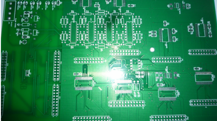
PCB circuit board processing
Hybrid Integrated Circuit
A circuit that applies precious metal conductive ink on a small ceramic thin substrate by printing, and then burns away the organic matter in the ink at high temperature, leaving a conductor circuit on the board surface, and can be used for welding of externally bonded parts. It is a circuit carrier attributed to thick film technology between the printed circuit board and the semiconductor integrated circuit device. In the early stage, it was used for military or high-frequency applications. In recent years, the price of the hybrid is very expensive and the military is declining, and it is not easy to automate production, coupled with the increasing miniaturization and refinement of circuit boards, the growth of this hybrid has been much worse than in the early years. .
Interposer
Refers to any two layers of conductors carried by an insulating object, and the place where it is to be connected is filled with some conductive fillers, which is called Interposer. For example, in the bare holes of the multilayer board, if it is filled with silver paste or copper paste to replace the orthodox copper hole wall, or the straight one-way conductive adhesive layer and other materials, all belong to this type of Interposer.
Laser Direct Imaging, LDI laser direct imaging
Instead of exposing the plate to the dry film for impression transfer, a computer is used to direct the laser beam to directly perform fast scanning photosensitive imaging on the dry film. Because what is announced is a single beam of parallel light with concentrated energy, the sidewall of the dry film after development can be made straighter. However, the method can only work on each board independently, so the mass production speed is far not as fast as the use of negatives and traditional exposure. LDI can only produce 30 medium-sized boards per hour, so it can only occasionally appear in prototypes or high-priced boards. Because of inherent high costs, it is difficult to promote in the industry.

Laser Maching
There are many fine processing in the electronics industry, such as cutting, drilling, welding, welding, etc., which can also be performed with the energy of laser light, which is called laser processing. The so-called LASER refers to the abbreviation of "Light Amplification Stimulated Emission of Radiation", which is translated as "laser" by the mainland industry, which seems to be more topical than transliteration. Laser was produced by the American physicist T.H. Maiman in 1959, using a single beam of light to hit the ruby to generate laser light. Years of research have invented a brand-new processing method. In addition to the electronics industry, it can also be used in medical and military applications.
Micro Wire Board micro-sealed wire (packet wire) board
The round cross-section enameled wire (glued-sealed wire) attached to the board surface is made into a special circuit board for PTH to complete the inter-layer interconnection. It is commonly called Multiwire Board "multi-wire board" in the industry. ), and the wire diameter is very small (below 25mil), also known as micro-sealed circuit board.
Moulded Circuit Molded three-dimensional circuit board
Using three-dimensional molds, injection molding (Injection Moulding) or transformation method to complete the three-dimensional circuit board manufacturing process, called Moulded circuit or Moulded Interconnection Circuit.
Multiwiring Board (or Discrete Wiring Board) multi-wire board
Refers to the use of ultra-fine enameled wires, three-dimensional cross wiring directly on the copper-free board surface, and then fixed with glue, drilling and plating, the obtained multilayer interconnection circuit board, called "multi-wire board ". This is developed by American PCK Corporation, and is still being produced by Nissan Hitachi. This kind of MWB can save planning time and is suitable for a small number of models with chaotic lines.
Noble Metal Paste
Conductive paste for thick film circuit printing. When it is printed on a porcelain substrate by a screen printing method, and then the organic carrier is burned away at a high temperature, a fixed precious metal circuit appears. The conductive metal particles used in this printing paste must be precious metals to prevent the formation of oxides at high temperatures. The products used are gold, platinum, rhodium, palladium or other precious metals.
Pads Only Board
In the early days of through-hole insertion, in some high-reliability multilayer boards to ensure solderability and circuit safety, only the through-holes and soldering rings were left outside the board, and the interconnection lines were hidden on the next inner layer. . Such two-layer boards will not be printed with solder resist green paint, they are particularly elegant in appearance, and the quality inspection is extremely strict. Now because of the increase in wiring density, many portable electronic products (such as mobile phones) have only SMT pads or a few lines left on the circuit board surface, and many dense interconnections are buried in the inner layer, and the layers are also changed. Difficult blind holes or "Pads On Hole" (Pads On Hole) are used as interconnections to reduce the damage of all-through holes to the ground and high-voltage copper surfaces. This type of SMT tightly mounted board is also only a backing board.
Polymer Thick Film (PTF) thick film paste
Refers to the ceramic substrate thick film circuit board, the precious metal printing paste used to make the circuit, or the printing paste that forms the printed resistive film. The process includes screen printing and subsequent high-temperature incineration. After the organic carrier is burned away, a strong and adherent circuit system appears. This type of board is generally called hybrid circuit board(Hybrid Circuits).
Semi-Additive Process
It means to directly grow the required circuit on the insulating substrate surface by chemical copper method, and then use electroplating copper method to continue thickening, which is called "semi-additive" process. If the chemical copper method is used for all circuit thicknesses, it is called a "full additive" process. The "D version" in the early stage and the general term in the industry refer to the non-conductor bare base material, or the thin copper foil (such as 1/4 oz or 1/8 oz) substrate. First prepare the impression of the negative resist, and then thicken the required circuit by chemical copper or copper electroplating. The new 50E does not mention the wording of thin copper skin. The distance between the two statements is quite large, and readers should also keep pace with the age in concept.
ipcb is a high-precision, high-quality PCB manufacturer, such as: isola 370hr PCB, high-frequency PCB, high-speed PCB, ic substrate, ic test board, impedance PCB, HDI PCB, Rigid-Flex PCB,buried blind PCB, advanced PCB, microwave PCB, telfon PCB and other ipcb are good at PCB manufacturing.