The internal structure of the PCB circuit board! Interpret the design process of high-end PCB boards!
When hardware engineers are new to multilayer PCBs, it is easy to get dizzy. There are ten and eight layers at every turn, and the lines are like spider webs.
The circuit processing of multilayer PCBs is no different from single-layer and double-layer. The biggest difference lies in the process of vias.
The lines are all etched, and the vias are all drilled and then plated with copper. Everyone who does hardware development understands these, so I won't go into details. If you don’t understand, you can look at the two articles before Yizhitoutiaohao.
PCB process article-1
PCB process article-2

multilayer PCBs usually include through-hole boards, first-level boards, second-level boards, and second-level stacked-hole boards. Higher-end boards, such as third-order boards and arbitrary-layer interconnect boards, are usually used very little and are expensive, so I won't discuss them first.
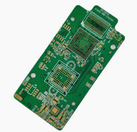
In general, 8-bit single-chip products use 2-layer through-hole boards; 32-bit single-chip-level smart hardware uses 4-layer-6-layer through-hole boards; Linux and Android-level smart hardware uses 6-layer through-hole to 8-level HDI board: Compact products such as smart phones generally use 8-layer first-order to 10-layer 2-layer circuit boards.
8-layer 2-step stacked hole, Qualcomm Snapdragon 624
The most common through holes
There is only one type of via, from the first layer to the last layer. Whether it is an external circuit or an internal circuit, the holes are punched through. It is called a through-hole plate.
Through-hole boards and the number of layers do not matter. Everyone usually uses two-layer through-hole boards, but many switches and military circuit boards do 20-layer through-hole boards.
Use a drill to drill through the circuit board, and then plate the hole with copper to form a via.
It should be noted here that the inner diameter of the through hole is usually 0.2mm, 0.25mm and 0.3mm, but generally 0.2mm is much more expensive than 0.3mm. Because the drill bit is too thin and easy to break, the drill is slower. The time spent and the cost of the drill bit are reflected in the increase in the price of the PCB boards.
Laser hole of high density board (HDI board)
The laminated structure diagram of the 6-layer 1-stage HDI board. Both layers on the surface are laser holes, with an inner diameter of 0.1mm. The inner layer is a mechanical hole
It is equivalent to a 4-layer through-hole board with 2 layers on the outside.
The laser can only penetrate glass fiber sheets, not metal copper. Therefore, the outer surface punching will not affect other internal circuits.
After the laser drills the hole, go to copper plating, and the laser via is formed.
Level 2 HDI board, two layers of laser holes
6-layer HDI board with 2-step staggered holes. Usually, people use 6 floors and 2 levels few, and most of them start with 8 floors and 2 levels. There are more layers here, the same as 6 layers
The so-called 2nd order means there are 2 layers of laser holes
The so-called wrong hole means that the two layers of laser holes are staggered.
Why should it be staggered? Because the copper plating is not full, the inside of the hole is empty, so you can't drill holes directly on it, you have to stagger a certain distance, and then make a layer of empty.
6 layers of second order = 4 layers of 1 order plus 2 layers outside.
8 layers of second order = 6 layers of 1 order plus 2 layers outside.
Stacked orifice plate, the process is more complicated and the price is higher.
The two layers of laser holes of the staggered hole plate overlap each other. The line will be more compact.
The inner laser hole needs to be electroplated and filled, and then the outer laser hole is made. The price is more expensive than the wrong hole.
Super expensive any layer interconnection board, multilayer laser stacking holes
That is, each layer is a laser hole, and each layer can be connected together. You can route the cables as you want, or punch as you want.
The layout engineer feels cool to think about it! Never be afraid of not being drawn anymore!
I just want to cry when I think about purchasing it, more than 10 times more expensive than ordinary through-hole boards!
Therefore, only products like the iPhone are willing to use it. For other mobile phone brands, I have never heard of anyone who has used any layer of interconnection PCB boards.