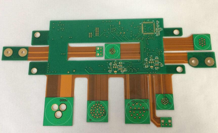
A revolutionary new process route for blind hole drilling of Rigid-Flex PCB, Current status of voids inflexible and rigid circuit boards.
Outside of mechanical drilling, we adopt a long-term perspective and only discuss laser drilling.
At present, carbon dioxide laser drilling is widely used in hard and flexible connecting plates, rather than in ultraviolet laser drilling.
The reason is that the holes of hard and flexible circuit boards are wide and extensive, which indicates that relatively high laser energy injection is required to achieve high-efficiency drilling. The power of the carbon dioxide laser can easily reach hundreds of watts, the beam quality is very good, and the power of the ultraviolet laser cannot be increased.
Carbon monoxide laser drilling is more suitable for high-efficiency drilling than ultraviolet laser drilling. However, the use of carbon dioxide lasers in drilling meets the requirements of high-energy injection.
The carbon dioxide laser has a high response to copper, and carbon dioxide drilling cannot directly affect the copper skin. Therefore, CO2 laser drilling is a problem.
It is necessary to further solve the problem of the copper film on the surface, that is, cover a special mask on the surface of the printed circuit board, and expose/develop the copper film through traditional methods.
The etching process removes the window formed from the surface of the hole from the surface of the copper foil. Subsequently, a carbon dioxide laser was used to irradiate these windows and eliminate the exposed resin layer. In short, carbon dioxide laser drilling provides the following means to overcome the copper barrier.

(1) How to open the bronze window. First, the RCC layer (resin-coated copper foil) is pushed onto the inner panel to fabricate the window with a photochemical method and then etched to expose the resin.
The laser is cut on the substrate in the window to form orgasm micro-holes. If the bottom plate (target) is not large enough, a large area or a secondary cannon is needed, then the accuracy of the window is difficult.
(2) The process of opening windows. In the first case, the diameter of the hole is the same as the diameter of the open copper window. If the operation is neglected slightly, opening the open window position will cause the empty hole position to move and make the bottom center out of the joint.
The deviation of the copper window can be attributed to the expansion and contraction of the base material and the deformation of the film used for image transmission.
Therefore, the opening process of the large copper window includes setting the diameter of the copper window to about 0.05 mm (usually determined by the size of the hole). When the diameter of the lower layer is 0.15 mm, the diameter of the bottom should be 0.15 mm. The diameter of the large window is about 0.25 mm and 0.30 mm.
Then it can be drilled with a laser to penetrate the micro-holes where the position is joined to the bottom. Its main feature is that the degree of freedom of choice is huge.
When laser drilling, you can drill according to the inner bottom pillow plan. This effectively avoids the deviation caused by the same diameter and hole formation of the copper window, so that the laser spot cannot be consistent with the regular window, and causes many incomplete half holes or residual holes on the large surface of the wholesale board.
(3) It is directly extracted from an ultra-thin film copper foil. After the two sides of the score sheet are covered with a resin copper foil, the copper foil can be reduced to 5 microns by a "half etching method" after the attack, and then treated with black oxidation. A CO2 laser can be used to form the hole.
The basic principle is that the oxidized black surface will directly absorb light so that by increasing the energy of the CO2 laser, holes on the surface of the ultra-thin film and resin can be directly formed.
But the most difficult thing is how to ensure that the "half etching process" can obtain a uniform thickness of the copper layer. Therefore, special attention must be paid to the manufacturing industry. Of course, copper (UTC) materials can be used. The thickness of the copper leaf is about 5 microns.
According to this type of plate processing, the following aspects are mainly used in the process: it mainly provides material suppliers with strict quality and technical indicators to ensure that the thickness of the dielectric layer varies between 5 microns and 10 microns.
Because only by providing the dielectric thickness of the resin-coated copper foil substrate and the laser energy that is the same as the precision and bottom-hole cleanliness, the insurance can be insured.
At the same time, during the monitoring process, we must adopt the best evacuation technical conditions to ensure that the bottom layer of the submarine cave after laser drilling is clean and there are no residual residues.
It has a positive impact on the quality of non-porous and non-porous electroplating and electroplating.
From the above introduction, we can see that traditional ultraviolet laser drilling is too powerless, too expensive, and too expensive to meet hardened and soft connecting plates. We have tried many methods to overcome the copper barrier so that Laser drilling becomes carbon dioxide.
Hard glued board for traditional drilling systems.
ipcb is a high-precision, high-quality PCB manufacturer, such as Isola 370hr PCB, high-frequency PCB, high-speed PCB, ic substrate, ic test board, impedance PCB, HDI PCB, Rigid-Flex PCB, buried blind PCB, advanced PCB, microwave PCB, Telefon PCB, and other ipcb are good at PCB manufacturing.