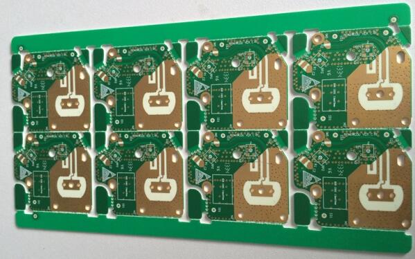
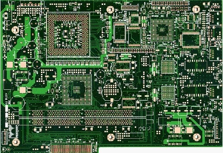
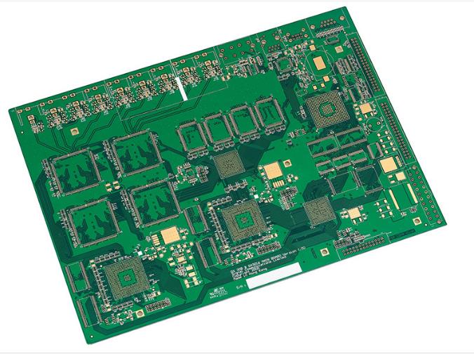
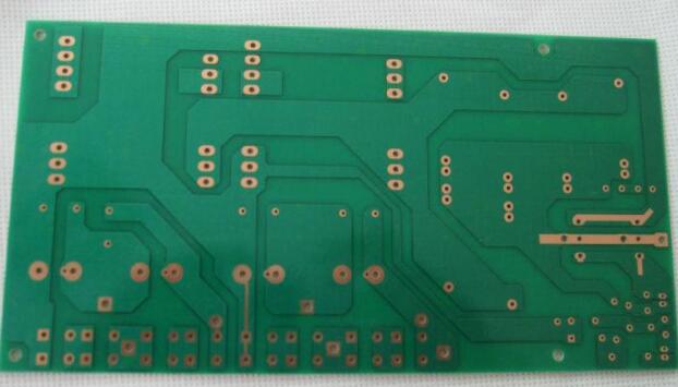
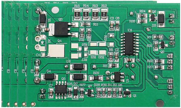
Talk about the basic principles of PCB stacking design
1. The second layer adjacent to the component surface is the ground plane, which provides the device shielding layer and the top layer wiring to provide a reference plane.
2. All signal layers are as close as possible to the ground plane to ensure a complete return path.
3. Try to avoid the two signal layers directly adjacent to reduce crosstalk.
4. The main power supply is as close as possible to it correspondingly to form a plane capacitor to reduce the plane impedance of the power supply.
5. Taking into account the symmetry of the laminated structure, it is conducive to the warpage control during plate making.
The above are the general principles of stacking design. In actual stacking design, circuit board designers can increase the distance between adjacent wiring layers and reduce the distance between the corresponding wiring layer and the reference plane to control the crosstalk rate of wiring between layers. It is possible to use two signal layers directly adjacent to each other.
For consumer products that pay more attention to cost, the way that the power supply and the ground plane are adjacent to the plane impedance can be weakened, so as to reduce the wiring layer as much as possible and reduce the PCB cost. Of course, the price of doing so is the risk of signal quality design.

For the backplane (Backplane or midplane) stacking design, in view of the common backplane it is difficult to achieve the adjacent traces perpendicular to each other, parallel long-distance wiring will inevitably appear. For high-speed backplanes, the general stacking principles are as follows:
1. Top surface and Bottom surface are complete ground planes, forming a shielded cavity.
2. There is no parallel wiring of adjacent layers to reduce crosstalk, or the distance between adjacent wiring layers is much larger than the reference plane distance.
3. All signal layers are as close as possible to the ground plane to ensure a complete return path.
It should be noted that in the specific PCB stacking settings, the above principles should be flexibly mastered and applied, and a reasonable analysis should be carried out according to the actual single board requirements, and finally a suitable stacking plan should be determined, and should not be mechanically applied.
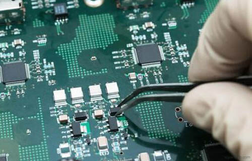
iPCB is happy to be your business partner. Our business goal is to become the most professional prototyping PCB manufacturer in the world. With more than ten years of experience in this field, we are committed to meeting the needs of customers from different industries in terms of quality, delivery, cost-effectiveness and any other demanding requirements. As one of the most experienced PCB manufacturers and SMT assemblers in China, we are proud to be your best business partner and good friend in all aspects of your PCB needs. We strive to make your research and development work easy and worry-free.
iPCB has passed ISO9001:2008, ISO14001, UL, CQC and other quality management system certifications, and produces standardized and qualified PCB products. We master complex process skills and use professional equipment such as AOI and Flying Probe to control production, X-ray inspection machines, etc. . Finally, we will use double FQC inspection of appearance to ensure shipment under IPC II standard or IPC III standard.