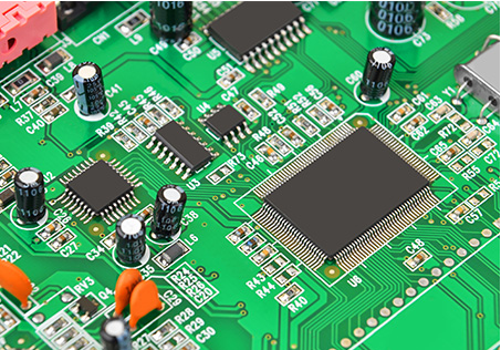
Selection of Micro-via Forming Technology for Printed Circuit Boards
The micro-vias on PCB circuit boards can be formed by a variety of production processes. The two longest methods used are laser etching process and mechanical equipment drilling. Which one to use should be determined by the specific regulations of the product.
This article gives a brief and detailed introduction to the laser etching process and mechanical drilling process to help the process technicians select the best application method according to their needs in the process of operating skills.
The micro-vias on PCB circuit boards are usually 0.002 inches (0.0 mm) to 0.008 inches (0.20 mm) in diameter. These vias can usually be divided into three types, namely blind holes, buried holes and through holes.
Blind holes are located on the top and bottom surface layers of the printed circuit board and have a certain depth. They are used to connect the surface route and the inner route below. The depth of the hole generally does not exceed the necessary ratio (aperture). Buried hole refers to the connection hole located in the inner layer of the printed circuit board, which does not easily extend to the surface of the PCB circuit board.
The above two types of holes are located in the inner layer of the PCB circuit board, and are completed by a through-hole forming process before lamination, and several outer films may be superimposed during the formation of the via. The third type is called a through hole. This kind of hole passes through the entire PCB circuit board and can be used for internal interconnection or as a mounting positioning hole for components.
Calculating the cost of micro-via technology should further measure the phenomena involved in each method, they are much more critical than the price of the facility.

When choosing a manual method for micro vias, the production cost per via is an important factor that should be considered.
In recent years, many applications have shown that the use of mechanical methods to make blind holes and through holes has made some progress and the cost is relatively low. Mechanical drilling technology In the past five years, advanced single-axis and multi-axis drilling systems have made a lot of progress.
Because of the use of finite element analysis and design, the stability of the machine has been improved a lot, and drilling equipment can be developed at a very fast speed, so that the performance of the machine can be quickly stabilized, thereby increasing the number of holes per minute.
Recently, a drill bit with an air bearing has been developed, which can rotate at more than 170krpm. In order to obtain a larger output during drilling, a higher speed is required, and the on-board measurement tool can monitor the status of the drill bit and the size of the hole.
At this stage, a new type of high-precision depth 1 control sensing technology for blind hole depth control is being developed. I think the key component of the pressure sensing probe uses the latest researched electric field sensing technology.
Each sensor signal is processed by a dedicated microprocessor, and it may be possible to process the signal of each controller in parallel, so that the bit status analysis is more rapid and accurate.
The principle is to detect the actual contact between the drill bit and the surface of the PCB circuit board, which enables the operator to control the drilling depth within the accuracy range of ±0.0002 inches (0.008mm).
Since the sensor detects the contact between the drill bit and the PCB circuit board, the accuracy will not be affected by the debris, board surface changes and surrounding burrs on the PCB circuit board. The sensor can monitor the data of the drill bit from 0.002 inch (0.05mm) to 0.250 inch (6.35mm) wear conditions within the range.
This type of technology is currently used in highly controlled micro-via drilling systems.
In addition, the drill bit is also changing. A special drill bit for blind hole processing is currently being developed. Engineering professionals are also trying to use grooved design and cemented carbide drill bits, hoping to improve the service life of precision long drill bits and reduce the production of each hole cost.
This is a uniquely designed drill that can be used to improve the forming of blind holes. Laser etching basically uses mechanical drilling when the aperture is larger than 0.008 inch (200um), while the smaller aperture is the key to laser drilling.
The minimum hole diameter of the laser drilling hole is 0.001 inch (25um). Generally speaking, the standard hole diameter is 0.004 inch (100um) to 0.006 inch (150um).
Until the end of 1999, laser drilling was only used in a few products. At that time, there were only 350 facilities in the world, and at least 300 of them were in Japan. They were all used in the first generation of laser drilling process: CO2 drilling without copper clad material. hole.
The number of laser drill holes will increase greatly in 2002, because the demand for mobile phones at that time is estimated to reach 350 million.
In order to produce enough printed circuit boards, 2,000 laser drilling equipment will be needed. This figure does not include the demand for small Internet access equipment, personal computers and other equipment.
The laser etching process drilling process includes direct dielectric drilling, conformal mask drilling and hole forming.
Immediate dielectric drilling is to irradiate the surface of the material with a CO2 laser beam. Each time a laser beam pulse is emitted, part of the material is etched away, and then the entire surface of the material is electroplated in the next step.
The characteristic of this processing technology is the fast drilling speed, but because the resolution of the CO2 laser is too low, the aperture cannot be less than 0.004 inches (100um); other uncoated materials also have problems such as coplanarity and accuracy. ipcb is a high-precision, high-quality PCB manufacturer, such as: isola 370hr PCB, high-frequency PCB, high-speed PCB, ic substrate, ic test board, impedance PCB, HDI PCB, Rigid-Flex PCB, buried blind PCB, advanced PCB, microwave PCB, telfon PCB and other ipcb are good at PCB manufacturing.