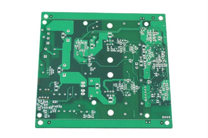
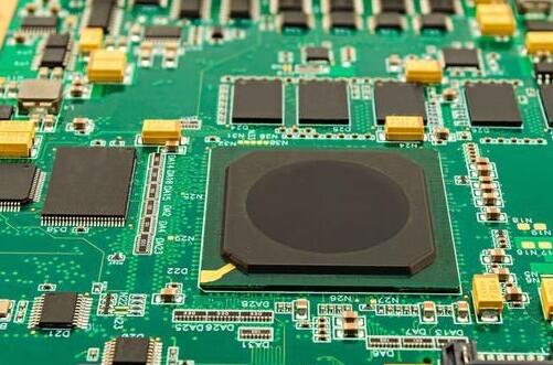
PCB circuit board characteristic impedance and resistance
PCB manufacturer: What is the characteristic impedance, the resistance generated by the alternating current in the component, which is related to the capacitance and inductance. When the electronic signal waveform is transmitted in the conductor, the resistance it receives is called the impedance resistance, which is the direct current in the component The resistance generated on the surface is related to voltage, resistivity,
Application of characteristic impedance
Mainly used for high-speed signal transmission and high-frequency circuits. The electrical performance provided by the printed boardmust be able to prevent reflection during signal transmission, keep the signal intact, reduce transmission loss, and play a matching role, so that it can be complete, Reliable, accurate, worry-free, and noise-free transmission signal impedance cannot be simply understood. The bigger the better or the smaller the better. The key is to match the control parameters of the characteristic impedance. The dielectric constant of the plate, the thickness of the dielectric layer, and the line width, Copper thickness, and the thickness of the solder mask. The influence of the dielectric constant of the plate is different from the control of the dielectric constant of different plates. It is related to the resin material used. The dielectric constant of FR4 plate is 4.2-4.7, which will increase or decrease with the frequency of use. Small, the dielectric constant of the PTFE sheet is between 2.9 and 3.9. The impedance value increases with the decrease of the dielectric constant. To obtain high signal transmission, a high impedance value is required, and a low dielectric constant is required.
Influence and control of dielectric layer thickness

Different prepregs have different glue content and thickness after pressing. The thickness after pressing is related to the flatness of the press and the pressing procedure.
For any kind of plate used, it is necessary to obtain the thickness of the medium layer that can be produced, which is conducive to the design calculation
The thickness of the dielectric layer is the most important factor affecting the impedance value
As it increases, the impedance value increases. The thickness deviation is controlled within 10% of the error
Influence and control of line width
The line width decreases, the impedance value increases
Within 10% tolerance required for line width control
The gap of the signal line affects the entire test waveform, and its single point impedance is too high, making the entire waveform uneven. The impedance line is not allowed to be patched, and the gap cannot exceed 10%
In order to ensure the line width, according to the amount of etching side etching, light drawing error, pattern transfer error, process compensation is performed on the engineering film to meet the line width requirements
Influence and control of copper thickness
The thicker the copper, the lower the impedance
To obtain a large impedance value, it is necessary to use a thin copper foil
The control of copper thickness is required to be uniform, and shunt blocks are added to the thin wires and isolated wires to balance the current to prevent uneven copper thickness on the wire and affect impedance
In the case of extremely uneven copper distribution on the cs and ss surfaces, the board should be crossed to achieve the goal of uniform copper thickness on both sides
The influence and control of solder mask
The thickness of the solder mask has little effect on the impedance. The thickness of the solder mask increases by 10um, and the impedance value changes only 1-2 ohms.
In the design, there is a big difference between the choice of cover and no cover solder mask, single-ended 2-3 ohms, differential 8-10 ohms
In the production of impedance boards, the thickness of the solder mask is normally controlled according to the production requirements
The degree of influence of each parameter
Copper thickness 8%, dielectric constant, 16%, solder resist thickness, 4%, line width, 24%, and dielectric layer thickness, 48%
Impedance test
CIT25nn tester
The basic method is the TDR method (time domain reflectometry). The basic principle is that the instrument emits a pulse signal, which is folded back through the test piece of the circuit board to measure the change in the characteristic impedance of the emission and the return. After computer analysis, the output characteristic impedance
Impedance problem handling
Regarding the control parameters of impedance, the control requirements can be achieved through mutual adjustment in production
After lamination in production, the board is sliced and analyzed. If the thickness of the medium is reduced, the line width can be reduced to meet the requirements; if the thickness is too thick, the copper can be thickened to reduce the impedance value
In the test, if there is a lot of difference between the theory and the reality, the biggest possibility is that there is a problem with the engineering design and the design of the test strip.
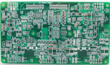
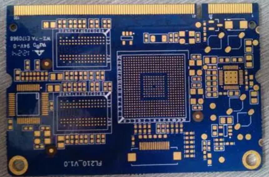
ipcb is a high-precision, high-quality PCB manufacturer, such as: isola 370hr PCB, high-frequency PCB, high-speed PCB, ic substrate, ic test board, impedance PCB, HDI PCB, Rigid-Flex PCB, buried blind PCB, advanced PCB, microwave PCB, telfon PCB and other ipcb are good at PCB manufacturing.