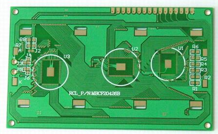
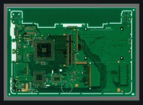
The process of making PCB board circuit board in circuit board factory The production of printed circuit boards is very complicated. Here, a four-layer printed circuit board is taken as an example to experience how the PCB board is made.
 laminated
A new raw material is needed here called a prepreg, which is the adhesive between the core board and the core board (PCB layer number>4), as well as the core board and the outer copper foil, which also plays a role in insulation. To
The lower copper foil and the two layers of prepreg have been fixed in advance through the alignment hole and the lower iron plate, and then the finished core board is also placed in the alignment hole, and finally the two layers of prepreg, a layer of copper foil and A layer of pressure-bearing aluminum plate covers the core plate.
The PCB boards clamped by the iron plates are placed on the support, and then sent to the vacuum heat press for laminating. The high temperature in the vacuum hot press can melt the epoxy resin in the prepreg and fix the core boards and copper foils together under pressure.
After the lamination is completed, remove the upper iron plate that presses the PCB board. Then take away the pressure-bearing aluminum plate. The aluminum plate also plays the role of isolating different PCB boards and ensuring the smoothness of the outer copper foil of the PCB board. Both sides of the PCB board taken out at this time will be covered by a layer of smooth copper foil.
drilling
To connect 4 layers of copper foils that are not in contact with each other in the PCB board, first drill through the through holes to penetrate the PCB board, and then metalize the hole walls to conduct electricity.
Use the X-ray drilling machine to locate the inner core board. The machine will automatically find and locate the holes on the core board, and then punch positioning holes on the PCB board to ensure that the next drilling is from the center of the hole. Through.
Put a layer of aluminum plate on the punching machine machine, and then put the PCB board on it. In order to improve efficiency, according to the number of layers of the PCB, 1 to 3 identical PCB boards are stacked together for perforation. Finally, a layer of aluminum plate is covered on the top PCB board. The upper and lower aluminum plates are used to prevent the copper foil on the PCB from tearing when the drill bit drills in and out.
In the previous lamination process, the molten epoxy was squeezed out of the PCB board, so it needs to be cut off. The profiling milling machine cuts its periphery according to the correct XY coordinates of the PCB board.
Chemical precipitation of copper on the hole wall
Since almost all PCB board designs use perforations to connect different layers of lines, a good connection requires a 25-micron copper film on the hole wall. The thickness of the copper film needs to be realized by electroplating, but the hole wall is composed of non-conductive epoxy resin and glass fiber board.
So the first step is to deposit a layer of conductive material on the hole wall, and form a 1 micron copper film on the entire PCB surface by chemical deposition, including the hole wall. The entire process such as chemical treatment and cleaning is controlled by the machine.
Outer PCB board layout transfer
Next, the outer PCB board layout will be transferred to the copper foil. The process is similar to the previous inner core board PCB board layout transfer principle, which is to transfer the PCB board layout to the copper foil using photocopied film and photosensitive film. The only difference is that positive films will be used for the board.
The internal PCB board layout transfer uses the subtractive method, and the negative film is used as the board. The PCB board is covered by the cured photosensitive film as a circuit, and the uncured photosensitive film is cleaned away. After the exposed copper foil is etched, the PCB layout circuit is protected by the cured photosensitive film.
The layout transfer of the outer PCB board adopts the normal method, and the positive film is used as the board. The non-circuit area is covered by the cured photosensitive film on the PCB. After cleaning the uncured photosensitive film, electroplating is performed. Where there is a film, it cannot be electroplated, and where there is no film, copper is plated first and then tin is plated. After the film is removed, alkaline etching is performed, and finally the tin is removed. The circuit pattern remains on the board because it is protected by tin.
The PCB board is clamped with clamps, and the copper is plated up. As mentioned earlier, in order to ensure adequate conductivity of the hole, the copper film plated on the hole wall must have a thickness of 25 microns, so the entire system will be automatically controlled by the computer to ensure its accuracy.
Outer PCB board etching
Next, a complete automated assembly line completes the etching process. First, clean the cured photosensitive film on the PCB board. Then use a strong alkali to clean the unnecessary copper foil covered by it. Then use the tin stripping solution to strip the tin plating on the copper foil of the PCB layout. After cleaning, the 4-layer PCB board layout is completed.