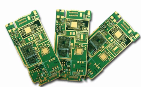
PCB circuit board pad size
The design in accordance with the pad requirements is to achieve the minimum diameter, which is at least 0.5mm larger than the maximum diameter of the solder terminal hole flange. Test pads must be provided for all nodes in accordance with the requirements of ANSI/IPC 2221. A node refers to two or The electrical connection point between multiple components. A test pad requires a signal name (node signal name, xy coordinate axis related to the reference point of the PCB circuit board, and the coordinate position of the test pad (indicating that the test pad is located on the PCB Which side of the circuit board, it is necessary to provide the information of the fixing device for the SMT, and the temperature bonding technology of the PCB circuit board assembly layout, in order to help in the "in-circuit test fixing device" or usually called the "nail bed fixing device" Promote testability in the circuit. In order to achieve this goal, it is necessary to:
1. The test pad should be placed in the center of a 2.5mm hole in a grid. If possible, allow the use of standard probes and a more reliable fixture.
2. Do not rely on the edge of the connector pointer for pad testing. The test probe can easily damage the gold-plated pointer.
3. Avoid probing on both sides of the plated through-hole-PCB circuit board. Put the test tip through the hole on the non-component/soldering surface of the PCB circuit board.

4. The diameter of the test pad dedicated to detection should not be less than 0.9mm.
5. The space around the test pad should be greater than 0.6mm and less than 5mm. If the height of the component is greater than 6.7mm, the test pad should be placed 5mm away from the component.
6. Do not place any components or test pads within 3mm from the edge of the PCB circuit board.
iPCB is a high-tech manufacturing enterprise focusing on the development and production of high-precision PCBs. iPCB is happy to be your business partner. Our business goal is to become the most professional prototyping PCB manufacturer in the world. Mainly focus on microwave high frequency PCB, high frequency mixed pressure, ultra-high multi-layer IC testing, from 1+ to 6+ HDI, Anylayer HDI, IC Substrate, IC test board, rigid flexible PCB, ordinary multi-layer FR4 PCB, etc. Products are widely used in industry 4.0, communications, industrial control, digital, power, computers, automobiles, medical, aerospace, instrumentation, Internet of Things and other fields.