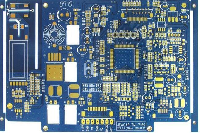
One of the high-speed PCB design guidelines
The first PCB layout
In PCB design, wiring is an important step to complete product design. It can be said that the previous preparations are done for it. In the entire PCB, the wiring design process has the highest limit, the finest skills, and the largest workload. PCB wiring includes single-sided wiring, double-sided wiring and multilayer wiring. There are also two ways of wiring: automatic wiring and interactive wiring. Before automatic wiring, you can use interactive to pre-wire the more demanding lines. The edges of the input end and the output end should be avoided adjacent to parallel to avoid reflection interference. If necessary, ground wire should be added for isolation, and the wiring of two adjacent layers should be perpendicular to each other. Parasitic coupling is likely to occur in parallel.
The routing rate of automatic routing depends on a good layout. The routing rules can be preset, including the number of bending times, the number of vias, and the number of steps. Generally, explore the warp wiring first, quickly connect the short wires, and then perform the labyrinth wiring. First, the wiring to be laid is optimized for the global wiring path. It can disconnect the laid wires as needed. And try to re-wire to improve the overall effect.
The current high-density PCB design has felt that the through-hole is not suitable, and it wastes a lot of valuable wiring channels. In order to solve this contradiction, blind and buried hole technologies have emerged, which not only fulfill the role of the through-hole It also saves a lot of wiring channels to make the wiring process more convenient, smoother, and more complete. The PCB board design process is a complex and simple process. To master it well, a vast electronic engineering design is required. Only when personnel experience it by themselves can they get the true meaning of it.

1 Treatment of power supply and ground wire
Even if the wiring in the entire PCB board is completed very well, the interference caused by the improper consideration of the power supply and the ground wire will reduce the performance of the product, and sometimes even affect the success rate of the product. Therefore, the wiring of the electric and ground wires must be taken seriously, and the noise interference generated by the electric and ground wires should be minimized to ensure the quality of the product.
Every engineer engaged in the design of electronic products understands the cause of the noise between the ground wire and the power wire, and now only the reduced noise suppression is described:
(1) It is well known to add a decoupling capacitor between the power supply and ground.
(2) Widen the width of the power and ground wires as much as possible, preferably the ground wire is wider than the power wire, their relationship is: ground wire>power wire>signal wire, usually the signal wire width is: 0.2~0.3mm, the most The slender width can reach 0.05~0.07mm, and the power cord is 1.2~2.5 mm
For the PCB of the digital circuit, a wide ground wire can be used to form a loop, that is, to form a ground net to use (the ground of the analog circuit cannot be used in this way)
(3) Use a large area of copper layer as the ground wire, and connect the unused places on the printed circuit board to the ground as the ground wire. Or it can be made into a multilayer board, and the power supply and ground wires occupy one layer each. 2 Common ground processing of digital circuit and analog circuit
Many PCBs are no longer single-function circuits (digital or analog circuits), but are composed of a mixture of digital and analog circuits. Therefore, it is necessary to consider the mutual interference between them when wiring, especially the noise interference on the ground wire. '
The frequency of the digital circuit is high, and the sensitivity of the analog circuit is strong. For the signal line, the high-frequency signal line should be as far away as possible from the sensitive analog circuit device. For the ground line, the whole PCB has only one node to the outside world, so The problem of digital and analog common ground must be dealt with inside the PCB, and the digital ground and analog ground inside the board are actually separated and they are not connected to each other, but at the interface (such as plugs, etc.) connecting the PCB to the outside world. There is a short connection between the digital ground and the analog ground. Please note that there is only one connection point. There are also non-common grounds on the PCB, which is determined by the system design.