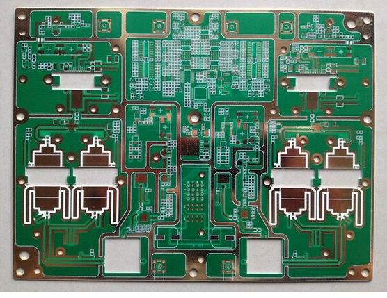
Characteristic impedance control circuit board process control
Circuit board factory: 1. Film production management and inspection
Constant temperature and humidity room (21±2°C, 55±5%), dustproof; line width process compensation.
2. Jigsaw design
The edges of the jigsaw panels should not be too narrow, the plating layer is uniform, and the electroplating adds false cathodes to disperse the current;
Design a coupon for the Z0 edge test on the jigsaw board.
3. Etching
Strict process parameters, reduce side corrosion, and conduct first inspection;
Reduce residual copper, copper slag, and copper scrap at the edge of the wire;
Check the line width and control it within the required range (± 10% or ± 0.02mm).

4. AOI inspection
The inner layer board must find wire gaps and protrusions. For 2GHZ high-speed signals, even 0.05mm gaps must be scrapped; controlling the inner layer line width and defects is the key.
5. Laminating
Vacuum laminator, reduce the pressure to reduce the flow of glue, try to keep as much resin as possible, because the resin affects the εr, the resin is stored more, and the εr will be lower. Control the tolerance of laminate thickness. Because the thickness of the plate is not uniform, it indicates that the thickness of the medium changes, which will affect Z0.
6. Choose the base material
Strictly cut the material according to the plate model required by the customer. The model is wrong, the εr is wrong, the board thickness is wrong, the PCB manufacturing process is all right, and the same is scrapped. Because Z0 is greatly affected by εr.
7. Solder mask
The solder mask on the board will reduce the Z0 value of the signal line by 1 to 3Ω. Theoretically, the solder mask thickness should not be too thick, but in fact the effect is not great. The surface of the copper wire is in contact with air (εr = 1), so the measured value of Z0 is higher. However, the Z0 value measured after the solder mask will drop by 1 to 3 Ω. The reason is that the εr of the solder mask is 4.0, which is much higher than that of air.
8. Water absorption
The finished multi-layer board should avoid water absorption as much as possible, because the water εr = 75, which will bring a great decline and unstable effect to Z0.
Six, summary
The characteristic impedance Z0 of the multi-layer board signal transmission line currently requires the control range to be: 50Ω±10%, 75Ω±10%, or 28Ω±10%.
To control the scope of change, four factors must be considered:
(1) Signal line width W;
(2) Signal line thickness T;
(3) The thickness of the dielectric layer H;
(4) Dielectric constant εr.
The biggest influence is the dielectric thickness, followed by the dielectric constant, the wire width, and the smallest is the wire thickness. After the substrate is selected, the change of εr is small, the change of H is also small, T is easier to control, but it is difficult to control the line width W at ±10%, and the line width problems include pinholes, notches, dents, etc. on the wire problem. In a sense, the most effective and important way to control Z0 is to control and adjust the line width.
iPCB is a high-tech manufacturing enterprise focusing on the development and production of high-precision PCBs. iPCB is happy to be your business partner. Our business goal is to become the most professional prototyping PCB manufacturer in the world. Mainly focus on microwave high frequency PCB, high frequency mixed pressure, ultra-high multi-layer IC testing, from 1+ to 6+ HDI, Anylayer HDI, IC Substrate, IC test board, rigid flexible PCB, ordinary multi-layer FR4 PCB, etc. Products are widely used in industry 4.0, communications, industrial control, digital, power, computers, automobiles, medical, aerospace, instrumentation, Internet of Things and other fields.