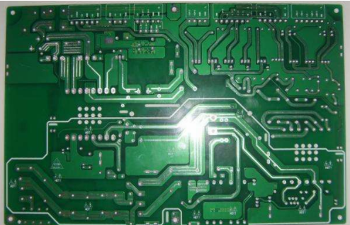
Via design of high-speed PCB
Through the analysis of the parasitic characteristics of vias, we can see that in high-speed PCB design, seemingly simple vias often bring great negative effects to circuit design. In order to reduce the adverse effects caused by the parasitic effects of the vias, the following can be done in the design:
1. The pins of the power supply and the ground should be drilled nearby, and the lead between the via and the pin should be as short as possible, because they will increase the inductance. At the same time, the power and ground leads should be as thick as possible to reduce impedance.
2. The two formulas discussed above can be concluded that using a thinner PCB is beneficial to reduce the two parasitic parameters of the via.
3. Try not to change the layers of the signal traces on the PCB board, that is to say, try not to use unnecessary vias.

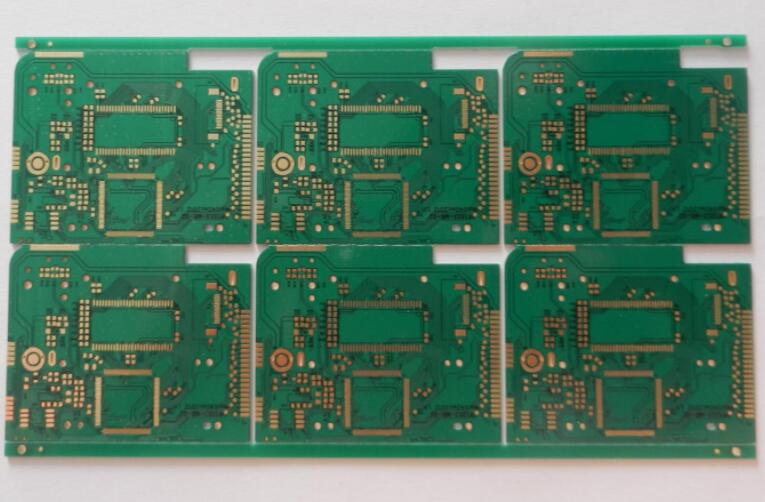
4. Considering the cost and signal quality, choose a reasonable size of the via hole. For example, for the 6-10 layer memory module PCB design, it is better to use 10/20Mil (drilled/pad) vias. For some high-density small-size boards, you can also try to use 8/18Mil. hole. Under current technical conditions, it is difficult to use smaller vias. For power or ground vias, you can consider using a larger size to reduce impedance.
5. Place some grounded vias near the vias of the signal layer to provide the nearest loop for the signal. It is even possible to place a large number of redundant ground vias on the PCB board. Of course, the design needs to be flexible. The via model discussed earlier is the case where there are pads on each layer. Sometimes, we can reduce or even remove the pads of some layers. Especially when the density of vias is very high, it may lead to the formation of a break groove that separates the loop in the copper layer. To solve this problem, in addition to moving the position of the via, we can also consider placing the via on the copper layer. The pad size is reduced.
iPCB is a high-tech manufacturing enterprise focusing on the development and production of high-precision PCBs. iPCB is happy to be your business partner. Our business goal is to become the most professional prototyping PCB manufacturer in the world. Mainly focus on microwave high frequency PCB, high frequency mixed pressure, ultra-high multi-layer IC testing, from 1+ to 6+ HDI, Anylayer HDI, IC Substrate, IC test board, rigid flexible PCB, ordinary multi-layer FR4 PCB, etc. Products are widely used in industry 4.0, communications, industrial control, digital, power, computers, automobiles, medical, aerospace, instrumentation, Internet of Things and other fields.