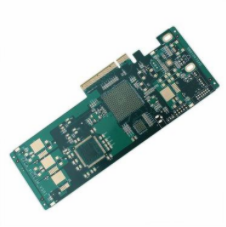
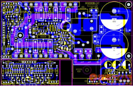
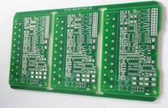
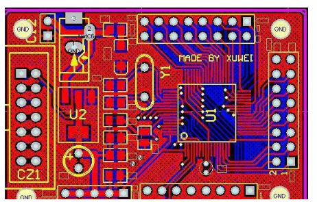
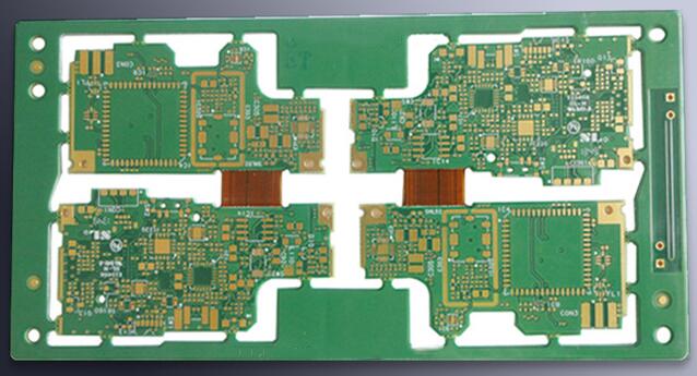
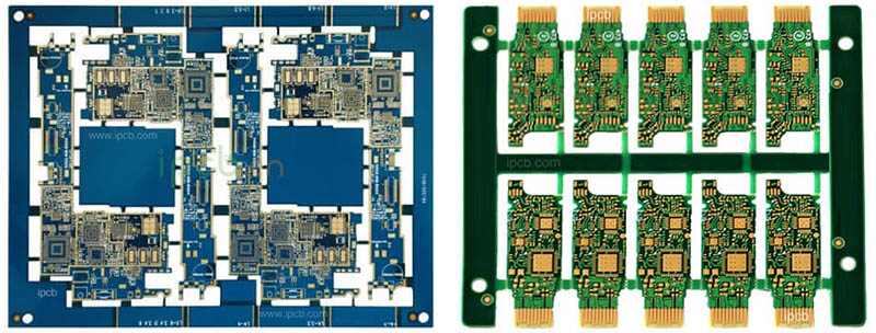
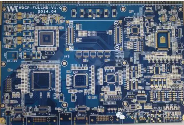
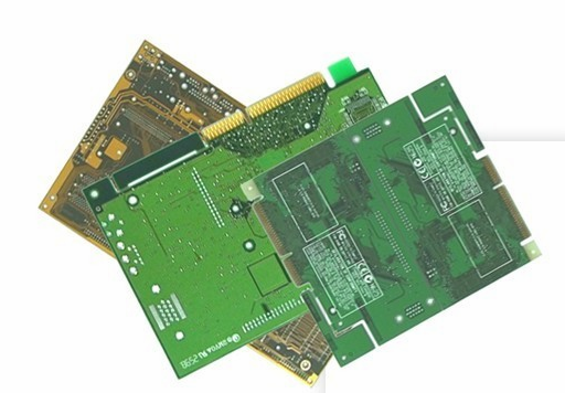
Multilayer board wiring experience
1. Consider the structure of component placement. The positive and negative poles of SMD components should be marked at the package and at the end to avoid space conflicts.
2. At present, the printed circuit board can be used for 4-5mil wiring, but it is usually 6mil line width, 8mil line spacing, 12/20mil pad. The wiring should consider the influence of sink current, etc.
3. After the wiring is completed, carefully check whether each connection line (including NETLABLE) is really connected (lighting method can be used).
4. The oscillating circuit components should be as close as possible to the IC, and the oscillating circuit should be as far away as possible from the antenna and other vulnerable areas. Place a ground pad under the crystal oscillator.

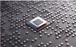
5. Consider multiple methods such as reinforcement and hollowing out components to avoid excessive radiation sources.
6. Put the functional block components together as much as possible, and the zebra strips and other components near the LCD should not be too close.
7. The lines between different layers should not be parallel as much as possible, so as not to form actual capacitance.
8. The wiring should be as straight as possible, or a 45-degree broken line, to avoid electromagnetic radiation.
9. It is best not to place pads, excessive air, etc. under the battery holder. The size of PAD and VIL is reasonable.
10. The ground wire and power wire are at least 10-15mil or more (for logic circuits).
11. Try to connect the grounding polylines together to increase the grounding area. Try to be as neat as possible between lines.
12. Pay attention to the uniform discharge of components to facilitate installation, plug-in, and welding operations. The text is arranged in the current character layer, the position is reasonable, pay attention to the orientation, avoid being blocked, and facilitate production.
13. The vias should be painted with green oil (set to negative double value).
14. Connect more than three points, try to let the line pass through each point in turn for easy testing, and keep the line length as short as possible.
15. Try not to put wires between the pins, especially between and around the pins of integrated circuits.
iPCB is a high-tech manufacturing enterprise focusing on the development and production of high-precision PCBs. iPCB is happy to be your business partner. Our business goal is to become the most professional prototyping PCB manufacturer in the world. Mainly focus on microwave high frequency PCB, high frequency mixed pressure, ultra-high multi-layer IC testing, from 1+ to 6+ HDI, Anylayer HDI, IC Substrate, IC test board, rigid flexible PCB, ordinary multi-layer FR4 PCB, etc. Products are widely used in industry 4.0, communications, industrial control, digital, power, computers, automobiles, medical, aerospace, instrumentation, Internet of Things and other fields.