Process standards of PCB manufacturers
First, the purpose:
Standardize printed circuit board process design, meet the requirements of printed circuit board manufacturability design, provide printed circuit board process design guidelines for hardware designers, and provide process review criteria for process personnel to review printed circuit board manufacturability.
2. Scope:
This specification specifies the process design requirements that hardware designers should follow when designing printed circuit boards, and is applicable to all printed circuit boards designed by the company.
3. Special definition:
Printed circuit board(PCB, printed circuit board):
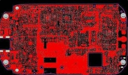
On an insulating substrate, a printed board with a printed element or a printed circuit or a combination of the two conductive patterns is formed according to a predetermined design.
Component Side:
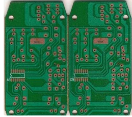
The side of the printed circuit board where the main components (main components such as IC) and most of the components are installed is characterized by complex components, which has a greater impact on the printed circuit board assembly process. Usually defined by the top surface (Top).

Solder Side:
The other side corresponding to the component side of the printed circuit board is characterized by simpler components. Usually defined by the bottom (Bottom).
Plated Through Hole:
A hole with metal deposited on the wall of the hole. Mainly used for electrical connection of conductive patterns between layers.
Unsupported hole:
There are no holes coated with electroplated layer or other conductive materials.
Lead hole (component hole):
The metalized holes on the printed circuit board used to electrically connect the leads of the components to the conductors of the printed circuit board.
Through hole:
The abbreviation for Hole Through Connection.
Blind via:
Multi-layer printed circuit board outer layer and inner layer conductive pattern electrical connection metallized hole.
Buried Via:
The metallized hole for the electrical connection of the conductive pattern between the inner layers of the multilayer printed circuit board.
Test hole:
Designed for electrical connection holes for printed circuit boards and printed circuit board components electrical performance testing.
Mounting holes:
refers to the mechanical fixing feet that pass through the components, and the holes that fix the components on the printed circuit board, which can be metalized holes or non-metalized holes, and the shape depends on the needs.
plug hole:
Block the through holes with solder mask ink.
Solder Mask, Solder Resist:
A coating used to provide dielectric and mechanical shielding during and after welding.
Pad (Land, Pad):
Conductive patterns for electrical connection and component fixing or both.
For other terms and definitions related to printed circuits, please refer to GB2036-80 "Printed Circuit Terms and Definitions".
Component Lead: A single or multiple stranded metal wire extending from the component as a mechanical connection or electrical connection, or a wire that has been formed.
Clinched Lead: The lead of the component is passed through the mounting hole of the printed board before soldering and then bent to form a lead.
Axial Lead: A lead extending along the axis of the component.
Wave Soldering: The soldering process in which the printed board is in contact with the continuous cycle of wave-like flowing solder.
Reflow Soldering: It is a soldering method in which the soldering end faces of the components and the PCB pads are coated with paste solder and then heated until the solder is melted, and then the soldering area is cooled.
Solder Bridging: The excess conductive path formed by solder between wires.
Solder Ball: A small ball formed by solder on the surface of a laminate, solder mask, or wire (usually after wave soldering or reflow soldering).
"Solder Projection": Excess solder bumps that appear on solidified solder joints or coatings.
Tombstone Component: A defect in which a double-ended chip component has only one metalized solder end soldered to the pad, and the other metalized solder end is raised and not soldered to the pad.
Integrated circuit package abbreviation:
BGA (Ball Grid Array): Ball grid array, a type of surface array package.
QFP (Quad Flat Package): Quad Flat Package.
PLCC (Plastic Leaded Chip Carrier): Leaded plastic chip carrier.
DIP (Dual In-line Package): Dual in-line package.
SIP (Single inline Package): Single inline package
SOP (Small Out-Line Package): Small outline package.
SOJ (Small Out-Line J-Leaded Package): J-lead small outline package.
COB (Chip on Board): Chip on board package.
Flip-Chip: flip chip.
Chip components (CHIP): Chip components are mainly passive components such as chip resistors, chip capacitors, and chip inductors. According to the different pins, there are full-terminal components (that is, component lead terminals covering the entire component end) and non-full-terminal components. General ordinary chip resistors and capacitors are full-terminal components, while tantalum capacitors are non-full-terminal components. element.
THT (Through Hole Technology): Through Hole Insertion Technology
SMT (Surface Mount Technology): Surface Mount Technology
4. Standard content:
There are many processing techniques in the electronic assembly process, including SMT, THT and SMT/THT mixed assembly. According to our company's characteristics, the following processing techniques are recommended:
Single-sided SMT (single-sided reflow soldering technology)
This kind of process is relatively simple. In a typical single-sided SMT, the main side of the PCB is all surface mount components (such as some of our memory products). According to the actual situation of our company, here we can slightly relax the single-sided SMT concept, that is, there can be a small number of THT components that meet the reflow soldering temperature requirements and through-hole reflow soldering conditions on the main side of the PCB, and these are soldered by through-hole reflow soldering technology. For THT components, taking into account the saving of steel mesh, it is also possible to allow a small number of SMT components on the other side to be manually soldered (such as some of our wireless network card products). The packaging requirements for manual soldering of SMT components are as follows:
For devices with lead spacing greater than 0.5mm (excluding 0.5mm), the package size of chip resistors and capacitors shall not be less than 0603, no 0402 resistance, no area array devices such as BGA. A small amount of THT components can also be welded manually.
The processing technology is: solder paste coating-component placement-reflow soldering-manual soldering
Double-sided SMT (Double-sided reflow soldering technology)
This kind of process is relatively simple (such as some of our memory products). It is suitable for PCBs with surface-mounted components on both sides, so surface-mounted components are required to be used as much as possible when selecting components to improve processing efficiency. If it is unavoidable to use a small part of THT components on the PCB, through-hole reflow soldering technology and manual soldering methods can be used. Using through-hole reflow soldering technology, THT components must meet the reflow soldering temperature requirements and through-hole reflow soldering conditions. Since this process is a secondary reflow soldering, during the second reflow soldering, the components at the bottom are adsorbed on the PCB by the surface tension of the molten solder. In order to prevent the heavy components from falling down or shifting when the solder is melted, there are certain requirements for the weight of the components on the bottom surface. The judgment basis is: the bearing weight of the contact surface of the solder fillet per square inch should be less than or equal to 30 grams. If the mesh belt type reflow soldering machine is used for welding, the device with a load-bearing contact surface of more than 30 grams per square inch must contact the mesh belt and keep the PCB board level with the mesh belt.
The processing technology is: solder paste coating-component mounting-reflow soldering-flipping board-solder paste coating-component mounting-reflow soldering-manual soldering
Single-sided SMT+THT mixed assembly (single-sided reflow soldering, wave soldering)
This kind of process is a commonly used processing method. Therefore, when PCB layout, the components should be placed on the same side as much as possible to reduce processing links and improve production efficiency.
The processing technology is: solder paste coating-component placement-reflow soldering-plug-in-wave soldering
Double-sided SMT+THT mixed assembly (double-sided reflow soldering, wave soldering)
This kind of process is more complicated, and it is common in our network products. The SMT components on the bottom of this kind of PCB board need to adopt a wave soldering process, so there are certain requirements for the SMT components on the bottom.
Area array devices such as BGA cannot be placed on the bottom surface, PLCC, QFP and other devices should not be placed on the bottom surface, fine-pitch lead SOP is not suitable for wave soldering, and chip components whose stand off cannot meet the printing requirements are not suitable for The printing glue is fixed, and it is not suitable to be placed on the bottom for wave soldering. The layout direction of the SOP device is also required. Please refer to the "Layout" section for specific requirements.
When designing such a PCB board with high component density, components must be arranged on the bottom surface and more THT components, this layout method is required to improve processing efficiency and reduce manual welding workload.
The processing technology is: solder paste coating-component placement-reflow soldering-flip board-printing glue-component placement-glue curing-flip board-plug-in-wave soldering
Component layout
General rules for component layout
Subject to design permission, the layout of components should be arranged in the same direction as much as possible, and modules with the same function should be arranged together; components of the same package should be placed at equal distances for component placement, soldering and testing .
PCB board size considerations
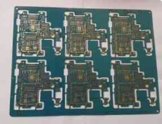
The key factor that limits the size of our PCB board is the processing capacity of the cutting machine.
When the milling cutter type cutting machine is involved in the selected processing technology, the PCB board size: 70mm*70mm-310mm*240mm.
When the round-knife cutting machine is involved in the selected processing technology, the PCB board size: 50mm*50mm (considering the processing capacity of other equipment)-450mm*290mm. Board thickness: 0.8mm-3.2mm.
When the selected processing technology does not involve the cutting machine (such as network products), the size of the PCB board: 50mm*50mm-457mm*407mm. (Wave soldering?), plate thickness: 0.5mm-3.0mm. See the appendix "Processing Equipment Parameter Table" for details. Special attention should be paid to the processing capacity of the equipment when making process fixtures.
Craft side
There must be at least one pair of edges on the PCB board with enough space for the conveyor belt, that is, the process edge. When PCB board is processed, the longer opposite side is usually used as the process side, which is reserved for the conveyor belt of the equipment. There should be no component and lead interference in the range of the conveyor belt, otherwise it will affect the normal transmission of the PCB board.
The width of the craft side is not less than 5mm. If the layout of the PCB board cannot be satisfied, you can use the method of adding auxiliary edges or jigsaw puzzles, see "Putting Boards".
PCB test impedance process side is greater than 7MM.
PCB board made of arc corners
Right-angled PCB boards are prone to jams during transmission. Therefore, when designing PCB boards, the board frame should be treated with arc corners, and the radius of the arc corners (5mm?) should be determined according to the size of the PCB board. The jigsaw and the PCB board with auxiliary edges are rounded on the auxiliary edges.
Safety distance between component bodies
Considering that there is a certain error when the machine is mounted, and considering the convenience of maintenance and visual appearance inspection, the two adjacent components should not be too close, and a certain safety distance should be left.
QFP, PLCC
The common feature of these two devices is the four-side lead package, the difference is that the lead shape is different. QFP is a gull wing lead, and PLCC is a J lead. Because it is a four-side lead package, the wave soldering process cannot be used.
QFP and PLCC devices are usually placed on the component side of the PCB. If they are to be placed on the soldering surface for the secondary reflow soldering process, their weight must meet the requirement that the weight of the contact surface of the solder fillet per square inch should be less than or equal to 30 grams.
BGA and other area array devices
BGA and other area array devices are used more and more. Generally, 1.27mm, 1.0mm and 0.8mm ball pitch devices are commonly used. The layout of area array devices such as BGA mainly considers its maintainability. Due to the space limitation of the hot air cover of the BGA rework station, there can be no other components within 3mm around the BGA. Under normal circumstances, area array devices such as BGA are not allowed to be arranged on the welding surface. When the layout space is limited, the area array devices such as BGA must be arranged on the welding surface, and their weight must meet the aforementioned requirements.
BGA and other area array devices cannot use wave soldering process.
SOIC device
There are many forms of small-outline packaged devices, such as SO, SOP, SSOP, TSOP, etc., and their common feature is the opposite-side lead package. Such devices are suitable for reflow soldering processes, and the layout design requirements are the same as those of QFP devices. The SOIC device with lead pitch ≥ 1.27mm (50 mil) and device standoff ≤ 0.15mm can adopt the wave soldering process, but pay attention to the relative direction of the SOIC device and the wave crest.
Standoff greater than 0.2mm can not cross the crest
SOT, DPAK device
SOT devices are suitable for reflow soldering process and wave soldering process, and can be placed on the component surface and the soldering surface during layout. When using the wave soldering process, the standoff of the device should be ≤0.15mm.