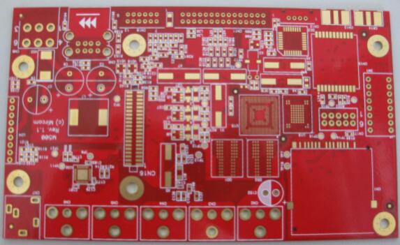
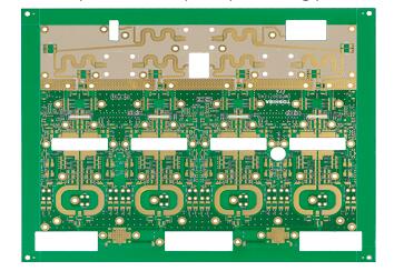
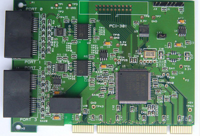
The copper wire of the PCB falls off
The PCB copper wire falls off (also commonly referred to as dumping copper).PCB factories all say that it is a laminate problem and requires their production factories to bear the bad losses. According to years of experience in handling customer complaints, the common reasons why PCB factories dump copper are as follows:
1. Reasons for laminate manufacturing process:
Under normal circumstances, as long as the laminate is hot pressed for more than 30 minutes, the copper foil and the prepreg will be basically completely combined, so the pressing will generally not affect the bonding force between the copper foil and the substrate in the laminate. However, during the process of stacking and stacking laminates, if the PP is contaminated or the matte surface of the copper foil is damaged, the bonding force between the copper foil and the substrate after lamination will also be insufficient, resulting in positioning (only for large plates) Words) or sporadic copper wires fall off, but the peel strength of the copper foil near the disconnected wires will not be abnormal.

2. Reasons for laminate raw materials:
1. As mentioned above, ordinary electrolytic copper foils are all products that have been galvanized or copper-plated on wool. If the peak value of the wool foil is abnormal during production, or when galvanizing/copper plating, the plating crystal branches are bad, causing the copper foil itself The peeling strength is not enough. After the bad foil pressed sheet material is made into a PCB, the copper wire will fall off when it is impacted by an external force when it is plugged in in the electronics factory. This kind of poor copper rejection will peel off the copper wire and look at the rough surface of the copper foil (that is, the surface in contact with the substrate). There will be no obvious side erosion, but the peel strength of the entire copper foil will be very poor.
2. Poor adaptability of copper foil and resin: some laminates with special properties, such as HTg sheets, are used now, because of different resin systems, the curing agent used is generally PN resin, and the resin molecular chain structure is simple. The degree of cross-linking is low, and it is necessary to use copper foil with a special peak to match it. When producing laminates, the use of copper foil does not match the resin system, resulting in insufficient peeling strength of the sheet metal-clad metal foil, and poor copper wire shedding when inserting.
Three, PCB factory process factors:
1. The copper foil is over-etched. The electrolytic copper foils used in the market are generally single-sided galvanized (commonly known as ashing foil) and single-sided copper plating (commonly known as red foil). Commonly thrown copper is generally galvanized copper above 70um. Foil, red foil and ash foil below 18um have basically no batch copper rejection. When the customer circuit design is better than the etching line, if the copper foil specifications are changed but the etching parameters remain unchanged, the residence time of the copper foil in the etching solution is too long. Because zinc is a kind of active metal, when the copper wire on the PCB is soaked in the etching solution for a long time, it will inevitably lead to excessive side corrosion of the circuit, causing some thin circuit backing zinc layer to be completely reacted and separated from the substrate. That is, the copper wire falls off. Another situation is that there is no problem with the PCB etching parameters, but the copper wire is also surrounded by the remaining etching solution on the PCB surface after the etching, and the copper wire is also surrounded by the residual etching solution on the PCB surface. Throw the copper. This situation is generally manifested as concentrated on thin lines, or during periods of wet weather, similar defects will appear on the entire PCB. Strip the copper wire to see that the color of the contact surface with the base layer (the so-called roughened surface) has changed. The color of the copper foil is different from the normal copper foil. The original copper color of the bottom layer is seen, and the peeling strength of the copper foil at the thick line is also normal.
2. A local collision occurred in the PCB process, and the copper wire was separated from the substrate due to external mechanical force. This poor performance is poor positioning or orientation, the copper wire will be obviously twisted, or scratches/impact marks in the same direction. If you peel off the copper wire at the defective part and look at the rough surface of the copper foil, you can see that the color of the rough surface of the copper foil is normal, there will be no side erosion, and the peeling strength of the copper foil is normal.
3. The PCB circuit design is unreasonable, and thick copper foil is used to design a circuit that is too thin, which will also cause excessive etching of the circuit and dumping of copper.