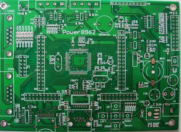
Design RF PCB matters
There are strict regulations on the width of the RF signal trace. When designing, it is necessary to strictly calculate and simulate the impedance of the trace at the corresponding frequency point according to the thickness and dielectric constant of the PCB to ensure that it is 50 ohms (the CATV standard is 75 ohms). However, not all of us need strict impedance matching all the time. In some cases, a small impedance mismatch may not be a big problem (for example, 40 ohms to 60 ohms); and even if your simulation of the board is based on Ideally, when it is actually delivered to the PCB factory for production, the process used by the manufacturer will cause the actual impedance of the board to differ from the simulation result by a thousand miles. Therefore, for the problem of impedance matching of small signal RF PCB, my suggestion is: Step-1: Properly communicate with the PCB factory to obtain the 50-ohm trace width range of the board with the corresponding thickness and the number of layers; Step-2: Choose an appropriate width within this width range and apply it uniformly to all 50-ohm RF signal lines; Step-3: When the PCB is delivered to production, indicate on the Script that all lines of this width are matched for 50-ohm impedance. At this point, there is no need to point out a lot of lines that need to be impedance matched (and for the PCB manufacturer, they will make an impedance bar in the form of imposition on the PCB extension of your design, and then leave it at the factory. When testing the impedance of a sample trace of the corresponding width on an impedance bar to roughly determine the impedance of the same width trace on the board. Finally, the impedance bar is cut off and recycled by the PCB factory, and will not be seen by you). And different frequencies, the impedance shown by the same width of the line

It will be slightly different, but the difference is generally within 10%. Of course, you can also write a very complicated impedance setting script, let the cardboard factory fine-tune the width of the traces working at different frequencies according to their process so that the impedance is strictly set to 50 ohms, and then ask the PCB factory to adjust each The root thread is screened. Doing so leads to a logarithmic increase in cost and a large scrap rate. Moreover, after the PCB is mounted, the impedance deviation will still be caused due to the solder distribution and the RF component itself. Such a situation is extremely rare, because even for precision RF test and measurement instruments, the error caused by the slight mismatch (within 5%) of the trace impedance of the RF small signal can be easily corrected by the software; and for the relatively rough As far as the telecommunications machine is concerned, you don’t even need to care about the 5% difference. But what I want to emphasize is that for the LNA (low noise amplifier) and PA (power amplifier) part of the RF circuit, the impedance of the RF trace is very sensitive, but fortunately, whether it is the LNA circuit or the PA circuit, the trace The frequency must be the same, and the number of wires is small (no more than two nodes, input and output). At this time, I suggest that in sensitive occasions, LNA and PA are made separately, and high-quality RF-specific PCB boards (Rogers/Arlon/Taconics) with uniform dielectric constant distribution are used. No solder mask is used in the RF signal line. Called green oil) to avoid impedance drift caused by solder mask; and require PCB board manufacturers to provide impedance test reports. Because the signal power of the input part of the LNA circuit itself is already very small (below -150dBm), the insertion loss caused by impedance mismatch further reduces the precious signal strength; for the PA circuit, because it works at a very high power, The insertion loss caused by impedance mismatch can consume a lot of energy (for comparison, the insertion loss is the same as 1dB: 10dBm signal attenuation is 9dBm and 50dBm attenuation is 49dBm, the difference in energy consumption, hehe, the latter can generate 20W of heat ) In some PAs with a power of over kilowatts, the insertion loss of 1dB may bring about the effect of splashing fire.
For those who implement the RF microstrip circuits generated by simulation in ADS, HFSS and other simulation tools on the PCB, especially those directional couplers, filters (PA narrowband filters), microstrip resonators (for example, you are designing VCO ), impedance matching network, etc., you must communicate well with the PCB factory, and use a sheet with strict specifications such as thickness and dielectric constant that are consistent with the specifications used in the simulation. The best solution is to find the agent of the microwave PCB board to buy the corresponding board, and then entrust the PCB factory to process it.
In RF circuits, we often use crystal oscillators as frequency standards. This crystal oscillator may be TCXO, OCXO or ordinary crystal oscillators. For such a crystal oscillator circuit must be far away from the digital part, and use a special low-noise power supply system. What's more important is that the crystal oscillator may drift in frequency with the change of the ambient temperature. For TCXO and OCXO, this situation will still occur, but the degree is smaller. Especially those small packaged crystal oscillator products are very sensitive to ambient temperature. For such a situation, we can add a metal cover to the crystal oscillator circuit (do not directly contact the crystal oscillator package) to reduce the sudden change of the ambient temperature and cause the frequency drift of the crystal oscillator. Of course, this will lead to an increase in size and cost.