PCB board and integrated circuit are not the same? What's the difference?
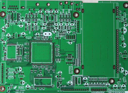
The current circuit boardmainly consists of the following:
1. Circuit and pattern (Pattern): The circuit is used as a tool for conduction between the originals. In the design, a large copper surface will be additionally designed as a ground and power layer. The route and the drawing are made at the same time.
2. Dielectric layer (Dielectric): used to maintain the insulation between the circuit and each layer, commonly known as the substrate.
3. Hole (Through hole / via): The through hole can make the lines of more than two levels connect to each other. The larger through hole is used as a part plug-in. In addition, there are non-through holes (nPTH) usually used as Surface mount positioning, for fixing screws during assembly.
4. Solder resistant /Solder Mask: Not all copper surfaces need to be tinned parts, so the non-tin area will be printed with a layer of material that isolates the copper surface from eating tin (usually epoxy resin), To avoid short circuits between non-tinned circuits. According to different processes, it is divided into green oil, red oil and blue oil.
5. Silk screen (Legend /Marking/Silk screen): This is a non-essential composition. The main function is to mark the name and position frame of each part on the circuit board, which is convenient for maintenance and identification after assembly.

6. Surface Finish: Because the copper surface is easily oxidized in the general environment, it can not be tinned (poor solderability), so it will be protected on the copper surface that needs to be tinned. The protection methods include HASL, ENIG, Immersion Silver, Immersion TIn, and OSP. Each method has its advantages and disadvantages, which are collectively referred to as surface treatment.
PCB board features
1. High-density: For decades, the high-density of printed boards has been able to develop along with the improvement of integrated circuit integration and the advancement of mounting technology.
2. High reliability: Through a series of inspections, tests and aging tests, the PCB can work reliably for a long time (usually 20 years).
3. Designability: For PCB performance (electrical, physical, chemical, mechanical, etc.) requirements, printed board design can be achieved through design standardization, standardization, etc., with short time and high efficiency.
4. Manufacturability: The use of modern management can carry out standardized, scaled (quantitative), automated and other production to ensure product quality consistency.
5. Testability: A relatively complete test method, test standard, various test equipment and instruments have been established to detect and appraise the eligibility and service life of PCB products.
Assemblability: PCB products are not only convenient for standardized assembly of various components, but also for automated and large-scale mass production. At the same time, PCB and various component assembly parts can be assembled to form larger parts and systems, up to the complete machine.