Many beginners feel that the Protel software itself is easy to learn and start with, but the more difficult to understand is some concepts and terms other than software. To promote this powerful EDA tool, manuals for the use of the software have been published domestically, but unfortunately, these books are often written for the use of the software itself, and there are few explanations for the concepts in the PCB process that confuse the reader. To design a suitable printed circuit board, you must first understand the general process flow of modern PCB, otherwise it will be a closed door car.
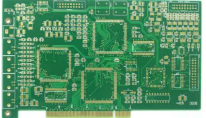
Generally speaking, there are one-sided, two-sided and multi-layer printing plates. The process of one-sided printing board is simple, usually blanking - screen leaking - etching - erasing - Printing - hole processing - printing marking - solder coating - finished product. The process of multi-layer printing board is more complex. That is: inner material treatment - positioning hole processing - surface cleaning treatment - making inner alignment and graphics - corrosion - layer pre-treatment - outer inner material layer - hole processing - hole metallization - making outer layer graphics - plating corrosion-resistant solderable metal - removing photosensitive gel - corrosion - plug gold plating - shape processing - hot melting - coating flux - forming Product. The process complexity of the double panel is somewhere in between, and is not discussed here.

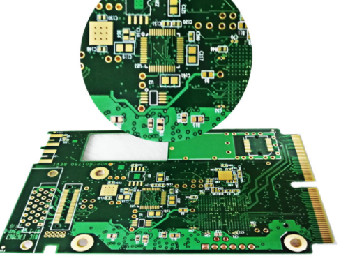
1. Concepts of PCB Layer
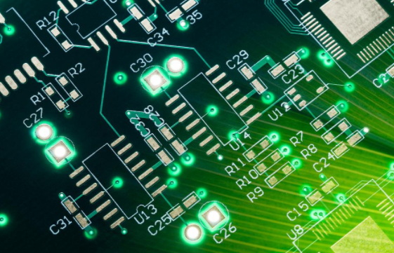
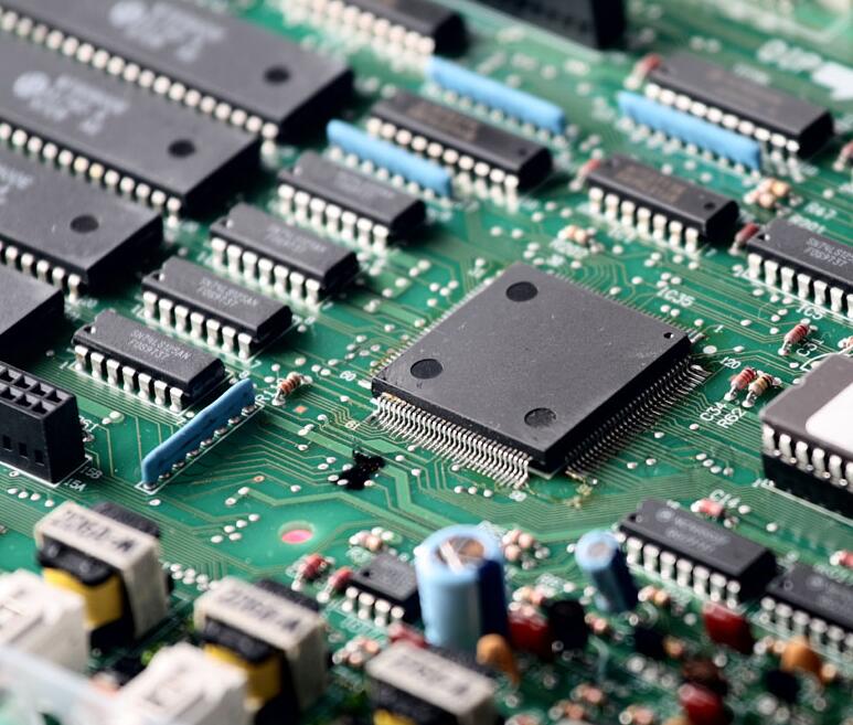
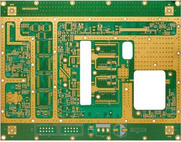
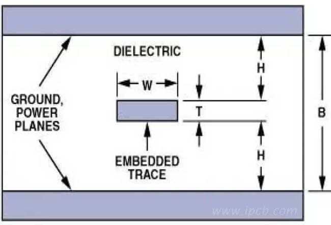
Unlike the concept of "layer" introduced in word processing or many other software for the nesting and synthesis of drawings, text, colors, etc., the "layer" of rotel is not virtual, but the real copper foil layers of the printed board material itself. Today, components of electronic circuits are installed intensively. For special requirements such as anti-interference and wiring, some newer electronic products use printed boards with not only upper and lower sides for wiring, but also sandwich copper foil which can be specially processed in the middle of the board. For example, computer motherboards now use more than four layers of printed board material. Most of these layers are used to set up power layers with simpler wiring, such as Ground Dever and Power Dever in the software, because they are relatively difficult to process, and wiring is often done by means of large area filling (such as ExternaI P1a11e and Fill in the software). Where the upper and lower surface layers and the middle layers need to be connected, the so-called "Via" mentioned in the software is used to communicate. With the above explanations, it is easy to understand the concepts of "multilayer pad" and "wiring layer setup". For example, many people finish wiring and find that many connected terminals do not have pads until they are printed out. In fact, this is because they ignore the concept of "layer" when adding the library of devices and do not define the pad characteristics of their own drawing package as "Mulii-Layer". It is important to note that once you have selected the number of layers to use, you must close those layers that are not used to avoid making any detours.
2. PCB Via
In order to connect the lines between layers, a common hole is drilled at the junction of the wires that need to be connected at each layer, which is called through hole. A layer of metal is chemically deposited on the cylindrical surface of the perforated hole wall to connect the intermediate layers of copper foil, and the upper and lower sides of the perforated hole are made into common bonding disc shapes, which can be directly connected or disconnected with the lines on both sides. Generally speaking, there are the following principles for the treatment of holes when designing lines:
(1) Minimize the use of holes. Once the use of holes is selected, it is important to handle the gap between holes and the surrounding entities, especially the gap between lines and holes that are easily overlooked and not connected by the middle layers. If the wiring is automatic, the on item can be selected in the Via Minimiz8tion sub-menu to solve the problem automatically.
(2) The larger the current carrying capacity required, the larger the size of the required holes, such as those used by the power layer and the stratum to connect with other layers.
3. PCB Overla
For the convenience of circuit installation and maintenance, the required logo patterns and text codes are printed on the upper and lower surfaces of the printed board, such as component labels and nominal values, component outline shapes and manufacturer's logos, production dates, etc. Many beginners only pay attention to the neat and beautiful placement of text symbols when designing the content of the screen printing layer, ignoring the actual PCB effect. On the printed board they designed, the characters were either blocked by components (such as riveted nuts) or credited for invading the welding aids, or the labels of the components were placed on adjacent components. All these designs would be inconvenient for assembly and maintenance. Correct Screen Layer Characters
The layout principle is "no ambiguity, seam insertion, beautiful and generous".
4. Particularity of SMD
There are a large number of SMD packages in the Protel package library, i.e. surface welded devices. In addition to its compact size, these devices are characterized by single-sided pin holes. Therefore, the selection of such devices should be well defined to avoid "Missing Plns". In addition, text labels for such elements can only be placed on the side of the element.
5. PCB Grid Filled Area (External Plane) and Fill Area (Fill)
As the names of both, the network filling area treats large areas of copper foil into a network, and the filling area only keeps the copper foil intact. Beginner design process in the computer often do not see the difference between the two, in essence, as long as you zoom in on the surface will be clear. It is because it is not easy to see the difference between the two, so we should pay less attention to the distinction between them when using. It should be emphasized that the former has a strong effect of suppressing high frequency interference on the circuit characteristics, and is suitable for large areas of filling, especially when some areas are used as shielding areas, partitions or power lines with large current.
The latter is used in general line ends or transition areas where small areas are needed to fill.
6. PCB Pad
Welding pad is a common and important concept in PCB design, but it is easy for beginners to ignore its selection and correction, and use circular pad consistently in the design. Selecting the type of pad for a component should take into account the shape, size, layout, vibration and acceptance of the component, force direction, etc. Protel gives a series of pads of different sizes and shapes in the encapsulation library, such as round, square, octagon, round and positioning pads, but sometimes this is not enough and needs to be edited by itself. For example, for a hot, high-force and high-current pad, it can be designed as "teardrop". In the design of pin pad of line-output transformer of color TV PCB, many manufacturers are familiar with this form. In general, in addition to the above, the following principles should be considered when editing the bond pads yourself:
(1) When the length is inconsistent in shape, the difference between the width of the connection and the specific side length of the pad should not be too large;
(2) It is often twice as useful to select asymmetric pads when traveling between the lead angles of components;
(3) The size of each component's pad holes should be determined according to the pin coarseness of the component. The principle is that the hole size is 0.2 - 0.4mm larger than the pin diameter.
7. PCB Mask
These membranes are not only indispensable in the process of PcB production, but also necessary for component bonding. Depending on the location of the "film" and its role, the "film" can be divided into component face (or welded face) welding aids (TOp or Bottom) and component face (or welded face) resistance (TOp or BottomPaste Mask) Two types. As the name implies, the solder film is a layer of film applied to the pad to improve solderability, that is, light spots slightly larger than the pad on the green plate. The opposite is true for the resistance film, which requires that the copper foil on the non-pad on the board should not be tin-bonded in order for the manufactured board to adapt to the form of wave soldering, so a layer of paint should be applied to all parts except the pad. Is used to prevent tin from being present on these sites. It is clear that these two membranes are a complementary relationship. From this discussion, it is not difficult to determine whether similar membranes are available in the menu.
Settings for items such as "solder Mask En1argement".
8. PCB Flight Line
A rubber band-like network connection for observation during automatic wiring, after elements have been imported through the network table and preliminary layout has been made, the wiring is "Show command can see the intersection of network connections under this layout, and constantly adjust the position of components to make this less intersection so as to obtain the wiring ratio of automatic wiring. This step is important, so to say, the sharpening knife does not cut firewood inaccurately, it takes some time, value! In addition, the end of automatic wiring, which networks are not connected, can also be found by this function. After the distribution network, manual compensation can be used, which really does not require the second meaning of "flying line". This means connecting these networks with wires on future printed boards. It is important to note that if the printed circuit board is manufactured in large quantities of automatic lines, such flylines can be designed as resistance elements with 0-ohm resistance and uniform pad spacing.