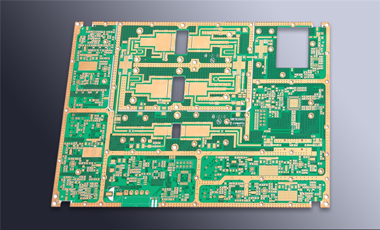
Printed circuit boards wiring plays a key role in high-speed circuits, but it is often one of the last steps in the circuit design process. There are many problems with high-speed PCB wiring, and a great deal of literature has been written on the subject. This paper mainly discusses the wiring problem of high-speed circuits from a practical point of view. The main purpose is to help new users become aware of the many different issues that need to be considered when designing PCB wiring for high-speed circuits. Another purpose is to provide a refresher material for customers who have not been exposed to PCB wiring for some time. Due to limited space, it is not possible to cover all of the issues in detail in this article, but we will discuss the key areas that are effective in improving circuit performance, reducing design time, and saving modification time.

Although the focus here is on circuits related to high speed operational amplifiers, the problems and methods discussed here are generally applicable to wiring for most other high speed analog circuits.When operational amplifiers operate in very high radio frequency (RF) bands, the performance of the circuit is largely dependent on PCB wiring. What appears to be a good high-performance circuit design on the "drawing board" will yield mediocre performance if it is affected by careless wiring. Pre-consideration and attention to important details throughout the wiring process will help ensure the desired circuit performance.
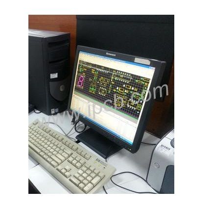
Schematic diagram
Although good schematics do not guarantee good wiring, good wiring starts with good schematics.The schematic diagram must be carefully drawn and the signal direction of the entire circuit must be considered. If you have normal, steady signal flow from left to right in the schematic, you should have just as good signal flow on the PCB. Give as much useful information as possible on the schematic. Because sometimes the circuit design engineer is not available, the customer will ask us to help solve the problem of the circuit. The designers, technicians and engineers who do this work will be very grateful, including us.
If you do not design your own wiring, be sure to allow plenty of time to double check the cabler's design. A little prevention is worth a hundred times a remedy here. Don't expect the cabling person to understand what you're thinking. Your input and guidance is important at the beginning of the wiring design process. The more information you can provide and the more involved you are in the wiring process, the better the PCB will be as a result. Set a tentative completion point for the cabling design engineer -- a quick check of the cabling progress you want. This "closed loop" approach prevents wiring from going astray and thus minimizes the possibility of rework.
Location
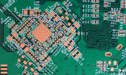
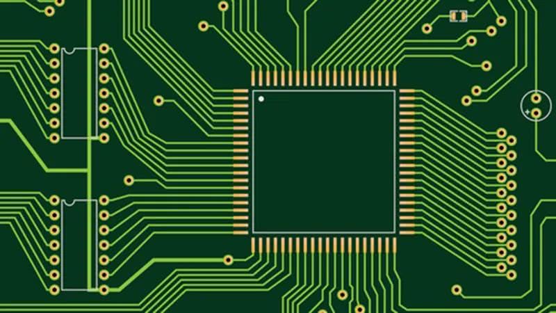
As in PCB, location is everything. Where a circuit is placed on the PCB, where its specific circuit components are installed, and what other circuits are adjacent to it are all very important.
Normally, the input, output and power supply positions are predetermined, but the circuitry between them needs to be "creative". This is why paying attention to the details of wiring can pay huge dividends. Start with the location of key components, consider the circuit and the entire PCB. Specifying the location of key components and the path of signals from the beginning helps ensure that the design works as intended. Getting the design right can reduce costs and stress -- and shorten development cycles.
Bypass the power supply
Bypassing the power side of the amplifier to reduce noise is an important aspect of the PCB design process -- both for high-speed operational amplifiers and other high-speed circuits. There are two common configurations of bypass high speed operational amplifiers. Power grounding: This method works in most cases, using multiple shunt capacitors to ground the power pins of the op amp directly. Two shunt capacitors are generally sufficient - but adding shunt capacitors may be beneficial for some circuits. Paralleling capacitors with different capacitance values helps ensure that the power supply pins see only low AC impedance over a wide band. This is especially important at the operational amplifier power rejection ratio (PSR) attenuation frequency. The capacitor helps compensate for the reduced PSR of the amplifier. Grounding paths that maintain low impedance over many tenx ranges will help ensure that harmful noise does not enter the operational amplifier. Figure 1 illustrates the advantages of using multiple shunt capacitors. At low frequencies, large capacitors provide low impedance ground access. But once the frequencies reach their resonant frequency, capacitors become less capacitive and take on more sensuality. This is why it is important to have multiple capacitors: as the frequency response of one capacitor begins to decline, the frequency response of the other capacitor comes into play, thus maintaining a very low AC impedance over many ten-octaves.
Conclusion
A high level of PCB wiring is important for successful operational amplifier circuit design, especially for high-speed circuits. A good schematic is the basis of good wiring; Close coordination between circuit design engineers and wiring design engineers is fundamental, especially with regard to the placement of components and wiring. Issues to be considered include bypass power supply, reducing parasitic effects, the use of grounding planes, the effects of operational amplifier packages, and wiring and shielding methods.
1. In PCB design, capacitor such as bypass filter at chip power supply should be as close to the device as possible, typical distance is less than 3MM.
The selection of capacitance values depends on the frequency of the input signal and the speed of the amplifier. For example, a 400MHz amplifier may use a 0.01uf and 1nF capacitor mounted in conjunction.
3. When we buy capacitors and other devices, we also need to pay attention to the self-resonant swing frequency, the self-resonant frequency in this frequency (400MHz) around the capacitor is not beneficial.
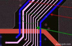
4. When drawing PCB, the input and output signal pins of the amplifier and the lower part of the feedback resistance should not run on other lines, so as to reduce the mutual influence of parasitic capacitance between different lines and make the amplifier more stable
5. The high frequency new energy of surface mount device is better and the volume is small
6. Circuit board wiring as short as possible, but also pay attention to his long and wide parasitic effect small
7. For the treatment of power cables, the parasitic characteristics of power cables are bad DC resistance and self-induction, so we try to widen the power cables as much as possible
8. For the amplifier, the current above the input/output line is very small, so they are easily affected. The parasitic effect is very harmful to them
9. For signal paths over 1CM, it is better to use a transmission line with controlled impedance and terminal (matching resistance) at both ends
10. Amplifier drive resistive and capacitive load To solve the problem of stability a common technique is to introduce a resistor ROUT close to the operational amplifier so as to achieve capacitive load isolation using series output resistors.