PCB hole copper thickness standard and finished copper thickness composition and origin
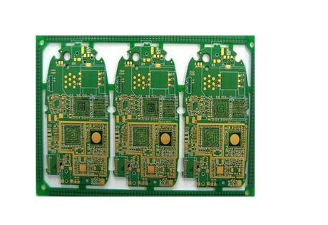
Not long ago, a small batch of PCB designed and manufactured by a customer was mounted in our PCBA factory. The mounting process was very smooth, but during the finished product test, 45% of defects were found, either without signal or just The signal is distorted.
After many days of investigation, it was finally found that the reason for the failure was that the copper thickness of the vias was uneven during the PCB production, and the copper of the PCB vias was too thin. As a result, the copper of the vias was affected by thermal shock during reflow soldering. Fracture, causing failure of open circuit.

The local copper thickness of the via hole is too thin and the via opening is one of the major technical issues faced by the PCB manufacturing industry. In the past, the discussion and research articles on the via opening are mostly limited to the selection of the board during the PCB manufacturing process, due to the CTE thermal expansion of the board. The coefficient is large, and the analysis of failure cases such as cracking of the hole copper caused by the hot and cold shock of the assembly in the later stage, instead of analyzing and solving the problem from the aspects of PCB processing and hole copper plating. This article analyzes the cause of partial copper thinness in the vias from the electroplating aspect of the PCB, and tells you how to avoid the PCB failure due to the open circuit due to the thin copper of the vias from the electroplating aspect.
Generally speaking, the copper standard pcb thickness of holes in traditional circuit boards is mostly required to be between 0.8-1 mil. As for some high-density circuit boards, such as HDI, because blind holes are not easy to electroplating and for the problem of thin wire production, it will moderately reduce the requirements for hole copper thickness. Therefore, there are also specifications with a minimum finished hole copper thickness of 0.4 mil or more. But there are also some special examples, such as: large circuit boards used in the system, because they have to deal with special assembly and long-term use of reliability guarantee, so the copper thickness in the hole is required to be higher than 0.8 mil or higher. In IPC-6012, there are clear grades for the thickness of the hole copper. Therefore, what kind of hole copper specification is required, according to the needs of the product, is ultimately specified by the customer.
Let’s go back to the case part at the beginning of our article. How can there be a failure of hole copper cracking? First of all, we must first understand the PCB production process.
The finished copper thickness of our PCB is based on the PCB base copper thickness plus the final thickness of the board and graphs, that is to say, the finished copper thickness is greater than the base copper of the PCB, and the copper thickness of all holes in our PCB is electroplated in two processes Completed, that is, the thickness of copper plated through holes and the copper thickness of pattern plating.
Our conventional finished product has a thickness of 1OZ finished copper, and the hole copper is in accordance with the IPC level II standard. We usually have a thickness of 5-7um for the first copper (full board plating) and 13-15um for the second copper, so the thickness of our hole copper is 18-22um In between, plus the loss caused by etching and other reasons, our final hole copper is about 20UM standard pcb thickness.