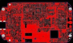
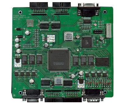
Improper PCB material and size will cause warpage and distortion
According to the regulations of GJB3835, after the warpage and distortion of PCBA during reflow soldering, the maximum bending and distortion should not exceed 0.75%, and the bow and distortion of PCB with fine-pitch components should not exceed 0.5%.
For PCBA with obvious warpage, if the multi-layer PCBA has deformation stress and then implement the anti-deformation installation (insertion) operations including reinforced metal frame installation, chassis platform screw installation, chassis guide slot insertion, etc., it is likely to cause High-density IC and other component leads, BGA/CCGA solder joints and multi-layer PCB relay holes and other printed conductor metallized holes are damaged or broken.
For PCBA whose distortion or bow has reached 0.75%, if it is confirmed that the deformation stress does not cause component damage and reliability problems and needs to continue to be used, it should be installed in accordance with the following relevant regulations.

It should not be directly installed (inserted) and screwed on the chassis platform, guide groove, guide rail or pillar, so as to avoid the anti-deformation stress of the printed circuit board assembly installation from further damaging the components and metallized holes.
Under the condition that the installation reliability is not affected and the main heat conduction path or main conduction path is ensured, local cushioning measures (electrical or heat-conducting materials) should be taken at the position where the gap between the distortion and bowing deformation is the largest. The warped parts can be installed and tightened only when the deformed printed circuit board assembly is not subjected to anti-deformation stress.
The rigidity and deformability of the materials selected for the PCB mounting structure and reinforcement frame should not cause distortion or bowing or anti-deformation of the PCB.
For multilayer PCBA with obvious distortion or bow, or distortion (bow) less than 0.75%, especially PCBA with high-density IC, BGA/CCGA components, it is necessary to strictly prevent the PCB from correcting or anti-deformation installation .
iPCB is a high-tech manufacturing enterprise focusing on the development and production of high-precision PCBs. iPCB is happy to be your business partner. Our business goal is to become the most professional prototyping PCB manufacturer in the world. Mainly focus on microwave high frequency PCB, high frequency mixed pressure, ultra-high multi-layer IC testing, from 1+ to 6+ HDI, Anylayer HDI, IC Substrate, IC test board, rigid flexible PCB, ordinary multi-layer FR4 PCB, etc. Products are widely used in industry 4.0, communications, industrial control, digital, power, computers, automobiles, medical, aerospace, instrumentation, Internet of Things and other fields.