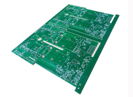
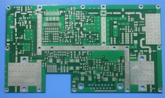
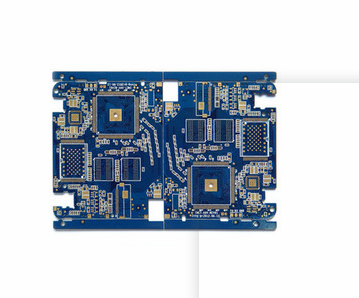
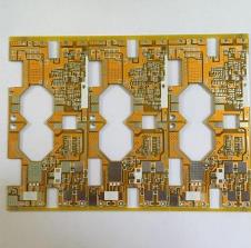
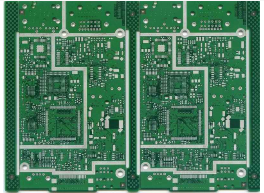
The production process of ordinary circuit boards is relatively simple, and the production process of multilayer circuit boards is relatively complicated. The following is a complete solution of the production process of multilayer circuit boards:

One, multilayer circuit board production process-lamination
1. Laminating is the process of bonding each layer of circuits into a whole by means of B-stage prepreg. This bonding is achieved through the mutual diffusion and penetration of macromolecules at the interface, and then interweaving. The process of bonding the various layers of circuits into a whole by the stage prepreg. This bonding is achieved through the mutual diffusion and penetration of macromolecules at the interface, and then interweaving.
2. Purpose: Press the discrete multi-layer board together with the adhesive sheet into a multi-layer board with the required number of layers and thickness.
1. The typesetting is to stack the copper foil, bonding sheet (prepreg), inner layer board, stainless steel, isolation board, kraft paper, outer layer steel plate and other materials according to the process requirements. If the board is more than six layers, pre-typesetting is required. Laminate copper foil, bonding sheet (prepreg), inner layer board, stainless steel, isolation board, kraft paper, outer layer steel plate and other materials according to the process requirements. If the board is more than six layers, pre-typesetting is required.
2. The laminated circuit board is sent to the vacuum heat press during the lamination process. The heat energy provided by the machine is used to melt the resin in the resin sheet, thereby bonding the substrate and filling the gap.
3. Lamination For designers, the first thing that needs to be considered for lamination is symmetry. Because the board will be affected by pressure and temperature during the lamination process, there will still be stress in the board after the lamination is completed. Therefore, if the two sides of the laminated board are not uniform, the stress on the two sides will be different, causing the board to bend to one side, which greatly affects the performance of the multilayer circuit board.
In addition, even in the same plane, if the distribution of copper is uneven, the resin flow speed at each point will be different, so that the thickness of the place with less copper will be slightly thinner, and the thickness of the place with more copper will be thicker. Some. In order to avoid these problems, various factors such as the uniformity of copper distribution, the symmetry of the stack, the design and layout of blind and buried vias, etc. must be carefully considered during the design.
Two, multilayer circuit board production process-the purpose of blackening and browning
1. Remove oil, impurities and other pollutants on the surface;
2. Increase the specific surface of the copper foil, thereby increasing the contact area with the resin, which is conducive to the full diffusion of the resin and the formation of a greater bonding force;
3. Make the non-polar copper surface into a surface with polar CuO and Cu 2 O, and increase the polar bond between the copper foil and the resin;
4. The oxidized surface is not affected by moisture at high temperatures, reducing the chance of delamination between the copper foil and the resin.
5. The board with the inner circuit must be blackened or browned before it can be laminated. It is to oxidize the copper surface of the inner board. Generally, the generated Cu 2 O is red and CuO is black. Therefore, the Cu 2 O-based oxide layer is called browning, and the CuO-based oxide layer is called blackening.
Three, multilayer circuit board production process-de-drilling and sinking copper
Purpose: Metallize the through hole
1. The substrate of the circuit board is composed of copper foil, glass fiber, and epoxy resin. In the manufacturing process, the hole wall section after the base material is drilled is composed of the above three parts of materials.
2. Hole metallization is to solve the problem of covering a uniform layer of copper with heat shock resistance on the cross section. Hole metallization is to solve the problem of covering a uniform layer of copper with heat shock resistance on the cross section.
3. The process is divided into three parts: one is the de-drilling process, the second is the electroless copper process, and the third is the thickening process (copper plating on the whole board).
Fourth, multilayer circuit board production process-outer dry film and pattern plating
The principle of outer layer pattern transfer is similar to that of inner layer pattern transfer, both using photosensitive dry film and photographing methods to print circuit patterns on the board. The difference between the outer dry film and the inner dry film is:
1. If the subtractive method is adopted, the outer dry film is the same as the inner dry film, and the negative film is used as the board. The cured dry film part of the board is the circuit. The uncured film is removed, and the film is retreated after acid etching, and the circuit pattern remains on the board because of the protection of the film.
2. If the normal method is adopted, the outer dry film is made of positive film. The cured part of the board is the non-circuit area (base material area). After removing the uncured film, pattern plating is performed. Where there is a film, it cannot be electroplated, and where there is no film, copper is plated first and then tin is plated. After the film is removed, alkaline etching is performed, and finally the tin is removed. The circuit pattern remains on the board because it is protected by tin.
3. Wet film (solder mask), the solder mask process is to add a layer of solder mask on the surface of the board. This layer of solder mask is called solder mask (Solder Mask) or solder mask ink, commonly known as green oil. Its function is mainly to prevent undesirable tinning of conductor lines, prevent short circuits between lines due to moisture, chemicals, etc., break circuits caused by poor operations in the production and assembly process, insulation, and resistance to various harsh environments, to ensure The function of the printed board, etc. Principle: At present, this layer of ink used by circuit board manufacturers basically uses liquid photosensitive ink. The production principle is partly similar to the transfer of line graphics. It also uses film to block the exposure and transfer the solder mask pattern to the PCB surface.
Five, multilayer circuit board production process-sink copper and thick copper
The metallization of holes involves a concept of capacity, the ratio of thickness to diameter. The thickness-to-diameter ratio refers to the ratio of the plate thickness to the hole diameter., Thickness to diameter ratio. The thickness-to-diameter ratio refers to the ratio of the plate thickness to the hole diameter. When the board continues to thicken and the hole diameter continues to decrease, it becomes more and more difficult for the chemical solution to enter the depth of the hole. Although the electroplating equipment uses vibration, pressure and other methods to allow the solution to enter the center of the hole, the center is caused by the difference in concentration. It is still unavoidable that the coating is too thin. At this time, there will be a slight open circuit phenomenon in the drilling layer. When the voltage increases and the board is impacted under various severe conditions, the defects are completely exposed, causing the circuit of the board to be disconnected and unable to complete the specified work.
Therefore, designers need to understand the process capability of the board manufacturer in time, otherwise the designed circuit board will be difficult to realize in production. It should be noted that the thickness-to-diameter ratio parameter must be considered not only in the design of through holes, but also in the design of blind and buried holes.