What are the defects caused by the common pad problem
At present, the country has higher and higher requirements for environmental protection and greater efforts in link governance. This is a challenge but also an opportunity for PCB factories. If PCB factories are determined to solve the problem of environmental pollution, then FPC flexible circuit board products can be at the forefront of the market, and PCB factories can get opportunities for further development.
The Internet era has broken the traditional marketing model, and a large number of resources have been gathered together to the greatest extent through the Internet, which has also accelerated the development speed of FPC flexible circuit boards, and then as the development speed accelerates, environmental problems will continue to appear in PCB factories. In front of him. However, with the development of the Internet, environmental protection and environmental informatization have also been developed by leaps and bounds. Environmental information data centers and green electronic procurement are gradually being applied to the actual production and operation fields. From this point of view, the environmental protection problems of PCB factories can be solved from the following two points.
1. Focus on product innovation in energy saving and emission reduction. PCB factories must learn to attach importance to Internet technology and realize the practical application of automated monitoring and intelligent management in production through the integration of overall industry knowledge.
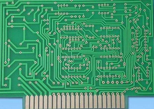
Common pads are a "common disease and frequently-occurring disease" in PCB design, and it is also one of the main factors that cause hidden dangers in PCB soldering quality.
After the chip components are soldered on the same pad, if the pin plug-in components or wiring are soldered again, there is a hidden danger of false soldering during the secondary soldering.
The number of repairs during subsequent commissioning, testing and after-sales maintenance is limited.
When repairing, unsoldering a component, the surrounding components of the same pad are all unsoldered.

When the pad is used in common, the stress on the pad is too large, causing the pad to peel off during soldering.
The same pad is shared between the components, the amount of tin is too much, the surface tension is asymmetric after melting, and the components are pulled to one side, causing displacement or tombstones.
Similar to the non-standard use of other pads, the main reason is that only the circuit characteristics are considered and the area or space is limited, which leads to a lot of component installation and solder joint defects in the assembly and welding process, which ultimately greatly affects the reliability of the circuit. Influence.
Our factory is located in China. For decades, Shenzhen has been known as the world's electronics R&D and manufacturing center. Our factory and website are approved by the Chinese government, so you can skip the middlemen and buy products on our website with confidence. Because we are a direct factory, this is the reason why 100% of our old customers continue to purchase on iPCB.
No minimum requirements
You can order as little as 1 PCB from us. We will not force you to buy things you really don't need to save money.
Free DFM
Before you pay in the most timely manner, all your orders will receive free engineering document review services by our well-trained professional and technical personnel.