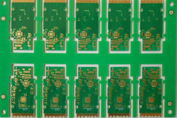
8-layer PCB circuit board proofing production process
A brief description of the difference between ordinary double-sided PCB board and multi-layer PC board:
The double-sided board is the middle layer of the medium, and both sides are the wiring layers. A multilayer board is a multilayer wiring layer. Between each two layers is a dielectric layer, which can be made very thin. Multilayer circuit boards have at least three conductive layers, two of which are on the outer surface, and the remaining layer is integrated into the insulating board. The electrical connection between them is usually achieved through plated through holes on the cross section of the circuit board.
8-layer PCB proofing production-the purpose of blackening and browning
1. Remove contaminants such as oil and impurities on the surface;
2. Increase the specific surface of the copper foil, thereby increasing the contact area with the resin, which is conducive to the full diffusion of the resin and the formation of greater bonding force;
3. Make the non-polar copper surface into a surface with polar CuO and Cu2O, and increase the polar bond between the copper foil and the resin;
4. The oxidized surface is not affected by moisture at high temperatures, reducing the chance of delamination between the copper foil and the resin.
5. The board with the inner circuit must be blackened or browned before it can be laminated. It is to oxidize the copper surface of the inner board. Generally, the produced Cu2O is red and CuO is black, so the Cu2O-based oxide layer is called browning, and the CuO-based oxide layer is called blackening.

1. Lamination is the process of bonding each layer of circuits into a whole by means of B-stage prepreg
This bonding is achieved through mutual diffusion and penetration between macromolecules at the interface, and then interweaving. The process of bonding the various layers of circuits into a whole by the stage prepreg. This bonding is achieved through mutual diffusion and penetration between macromolecules at the interface, and then interweaving.
2. Purpose: Press the discrete multi-layer board together with the bonding sheet into a multi-layer board with the required number of layers and thickness
1. Typesetting is to laminate copper foil, bonding sheet (prepreg), inner layer board, stainless steel, isolation board, kraft paper, outer layer steel plate and other materials according to the process requirements. If the board is more than six layers, pre-typesetting is required. Lay copper foil, bonding sheet (prepreg), inner layer board, stainless steel, isolation board, kraft paper, outer layer steel plate and other materials according to the process requirements. If the board is more than six layers, pre-typesetting is required.
2. The laminated circuit board is sent to the vacuum heat press during the lamination process. The heat energy provided by the machine is used to melt the resin in the resin sheet, thereby bonding the substrate and filling the gap.
3. Lamination For designers, the first thing that needs to be considered for lamination is symmetry. Because the board will be affected by pressure and temperature during the lamination process, there will still be stress in the board after the lamination is completed. Therefore, if the two sides of the laminated board are not uniform, the stress on the two sides will be different, causing the board to bend to one side, which greatly affects the performance of the PCB. Keyou Circuits specializes in the production of high-precision multilayer circuit boards. Products are widely used in: LCD liquid crystal modules, communication equipment, instrumentation, industrial power supplies, digital, medical electronics, industrial control equipment, LED modules/modules, power energy, transportation, High-tech fields such as science and education research and development, automobiles, aerospace and aviation. In addition, even in the same plane, if the distribution of copper is uneven, the resin flow speed at each point will be different, so that the thickness of the place with less copper will be slightly thinner, and the thickness of the place with more copper will be thicker. Some. In order to avoid these problems, various factors such as the uniformity of copper distribution, the symmetry of the stack, the design and layout of blind and buried vias, etc. must be carefully considered during the design.