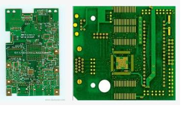
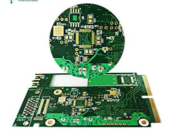
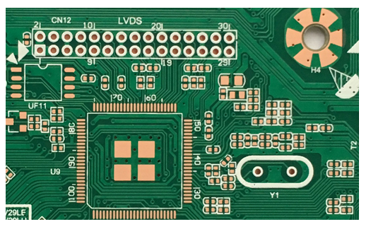
How to reduce the tin ball and tin dross on the PCBA board surface
In the PCBA processing process, due to the process and manual operation factors, there is a high probability that occasional tin balls and dross remain on the PCBA board surface, which causes great hidden dangers to the use of the product, because the tin balls and tin dross are in Loosening occurs in an uncertain environment, forming a short circuit of the PCBA board, resulting in product failure. The key is that this probability of occurrence is likely to appear in the life cycle of the product, which will cause great pressure on the customer's after-sales service.
The root cause of PCBA tin ball tin dross
1. There is too much tin on the SMD pad. During the reflow soldering process, the tin is melted and the corresponding tin bead is extruded.
2. The PCB board or components are damp, the moisture will explode during reflow soldering, and the splashed tin beads will be scattered on the board surface.
3. During the post-welding operation of DIP plug-in, the tin bead splashed from the tip of the soldering iron is scattered on the PCBA board surface when the tin is added by hand and the tin is shaken.
4. Other unknown reasons.
Measures to reduce PCBA tin beads and dross

1. Pay attention to the production of stencils. It is necessary to adjust the size of the opening appropriately in combination with the specific component layout of the PCBA board, so as to control the printing volume of the solder paste. Especially for some dense foot components or board surface components are denser.
2. For bare PCB boards with BGA, QFN and dense-foot components on the board, strict baking is recommended to ensure that moisture on the pad surface is removed, to maximize solderability and prevent the generation of tin beads.
3. PCBA processing manufacturers will inevitably introduce hand welding stations, which requires strict management control over tin dumping operations. Arrange a special storage box, clean the table in time, and strengthen the post-welding QC to visually inspect the SMD components around the manually welded components, focusing on checking whether the solder joints of the SMD components are accidentally touched and dissolved or the tin beads and tin dross are scattered to the yuan Between device pins.
PCBA board is a more precise product component, which is very sensitive to conductive objects and ESD static electricity. In the PCBA process, the managers of the factory need to improve the management level (recommended at least IPC-A-610E Class II), strengthen the quality awareness of the operators and the quality team, and implement it from the two aspects of process control and ideological awareness, to the greatest extent Avoid the production of tin balls and dross on the PCBA board surface.
Previous:Causes of soldering cracks in PCBA patches Next:How to control solder paste printing in PCBA processing