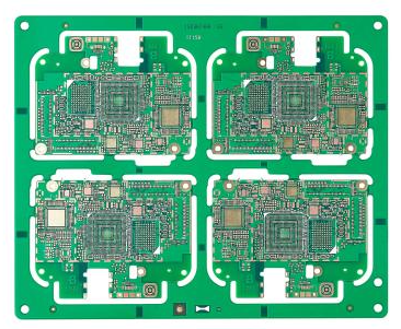
What is the production process of SMT patch processing template?
At present, the country has higher and higher requirements for environmental protection and greater efforts in link governance. This is a challenge but also an opportunity for PCB factories. If PCB factories are determined to solve the problem of environmental pollution, then FPC flexible circuit board products can be at the forefront of the market, and PCB factories can get opportunities for further development.
The Internet era has broken the traditional marketing model, and a large number of resources have been gathered together to the greatest extent through the Internet, which has also accelerated the development speed of FPC flexible circuit boards, and then as the development speed accelerates, environmental problems will continue to appear in PCB factories. In front of him. However, with the development of the Internet, environmental protection and environmental informatization have also been developed by leaps and bounds. Environmental information data centers and green electronic procurement are gradually being applied to the actual production and operation fields. From this point of view, the environmental protection problems of PCB factories can be solved from the following two points.
What is the standard of Mark's solution process?

1. Mark processing method, whether it is necessary to mark, put it on the side of the template and so on.
2. Which side of the template is placed on the Mark pattern should be determined according to the actual structure of the printing equipment (the location of the surveillance camera).
3. Mark dot engraving method depends on the printing equipment, including packaging printing surface, non-package printing surface, double-sided half-engraving, full-engraving and sealing vinyl, etc.
2. Is it the way to join the board, and its rules? If the board is joined, the PCB document of the board should be obtained.
3. Regulations for inserting weld layer ring. Because when the reflow soldering process is used for plug-in electronic devices, there is a larger amount of solder paste than that for mounted electronic devices. Therefore, if there are plug-in electronic devices that must be used for reflow soldering, special requirements can be specified.
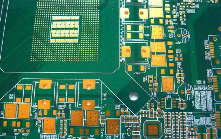
4. Modifications to the specifications and appearance of the template (welding layer) opening. Generally speaking, for the solder layer exceeding 2mm, in order to avoid the solder paste pattern from sinking and prevent tin beading, the opening of the "railway bridge" method is used. The graphic limit is 0.4mm, so that the opening is less than 2mm, which can be divided equally according to the size of the solder layer. . Various components stipulate the thickness and opening specifications of the template.
1. The square opening for μBGA/CSP and FlipChip is more cost-effective than the packaging and printing with circular opening.
2. When applying no-cleaning solder paste and selecting no-cleaning processing technology, the opening specification of the template should be reduced by 5% to 10%.
3. The opening design of the non-heavy metal processing technology template is larger than that with lead, and the solder paste should completely cover the solder layer as much as possible.
3. A moderate opening can improve the actual effect of SMT patch processing. For example, when the specifications of Chip PCB components are lower than 1005 metric and imperial systems, because the distance between the two solder layers is not large, the solder paste on the solder layers on both sides of the chip is very easy to adhere to the bottom of the component, and then flow soldering It is very easy to cause bridging and solder balls at the bottom of the components. Therefore, in the production and processing of the template, the inner side of the opening of the solder layer of a pair of rectangular frames can be changed into a bevel or bow shape to reduce the amount of solder paste at the bottom of the component, which can improve the soldering sound adhesion at the bottom of the component when the chip is mounted. The actual modification plan can be clarified by referring to the material of the "Printing Solder Paste Template Opening Design Plan" of the template manufacturer.