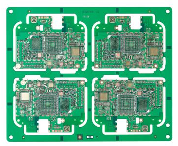
The board thickness and copper thickness issues that need to be considered in the design of double-layer PCB circuit boards
There are many issues that need to be considered in the design of double-layer PCB circuit boards. The following are the board thickness and copper thickness issues that need to be considered in the design of double-layer PCB circuit boards.
Cutting material mainly considers the board thickness and copper thickness:
The standard series of plates with a thickness of more than 0.8MM are: 1.0 1.2 1.6 2.0 3.2 MM, and the thickness of a plate less than 0.8MM is not considered as a standard series. The thickness can be determined according to needs, but the commonly used thicknesses are: 0.1 0.15 0.2 0.3 0.4 0.6MM, this material is mainly used for the inner layer of multilayer boards.
When designing the outer layer, pay attention to the thickness of the board. The production and processing need to increase the thickness of copper plating, solder mask thickness, surface treatment (tin spraying, gold plating, etc.) thickness, characters, carbon oil and other thickness. The actual production of sheet metal will be thicker than 0.05-0.1MM, The tin plate will be thicker than 0.075-0.15mm. For example, when the finished product requires a thickness of 2.0 mm during the design, when the 2.0mm sheet is normally selected for cutting, the thickness of the finished sheet will reach 2.1-2.3mm, taking into account the tolerance of the sheet and the processing tolerance. In the meantime, if the design requires that the thickness of the finished plate should not be greater than 2.0mm, the plate should be made of 1.9mm unconventional plate material. The double-layer PCB circuit board processing plant needs to temporarily order from the plate manufacturer, and the delivery cycle will become very short. long.

When the inner layer is made, the thickness after lamination can be adjusted by the thickness and structure configuration of the prepreg (PP). The choice of the core board can be flexible, for example, the thickness of the finished board is 1.6mm, and the choice of the board (core board) can be 1.2 MM can also be 1.0MM, as long as the thickness of the laminated plate is controlled within a certain range, the thickness of the finished plate can be met.
The other is the board thickness tolerance. When considering product assembly tolerances, designers of double-layer PCB circuit boardsmust also consider the thickness tolerances of the double-layer PCB circuit boards after processing. There are three main aspects that affect the tolerances of the finished product: sheet material tolerance and lamination. Tolerance and outer thickening tolerance. Several conventional sheet tolerances are now provided for reference: (0.8-1.0)±0.1 (1.2-1.6)±0.13 2.0±0.18 3.0±0.23 The lamination tolerance is controlled within ±(0.05-0.1) according to different layers and thicknesses MM. Especially for boards with board edge connectors (such as printed plugs), the thickness and tolerance of the board need to be determined according to the requirements of matching with the connector.
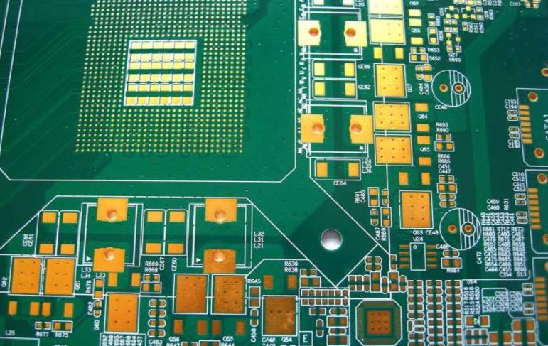
The surface copper thickness problem, because the hole copper needs to be completed by chemical copper plating and copper electroplating, if no special treatment is done, the surface copper thickness will be thicker when the hole copper is thickened. According to the IPC-A-600G standard, the minimum copper plating thickness is 20um for level 1, 2 and 25um for level 3. Therefore, if the copper thickness is required to be 1OZ (minimum 30.9um) when making the circuit board, the cutting may sometimes Choose HOZ (minimum 15.4um) cutting material according to the line width/line distance, remove the allowable tolerance of 2-3um, the smallest can reach 33.4um, if you choose 1OZ cutting, the minimum thickness of the finished copper will reach 47.9um. Other copper thickness calculations are available And so on.