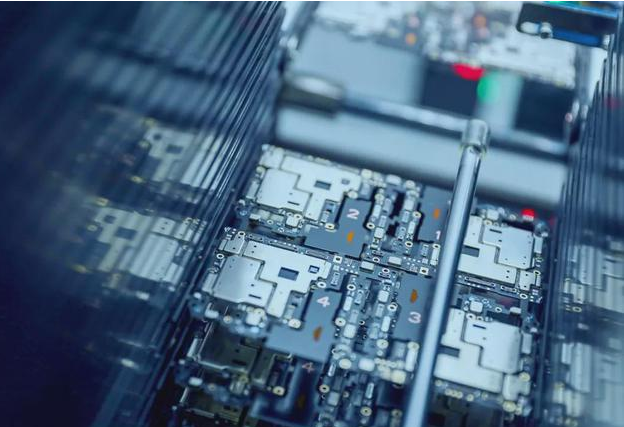
PCB manufacturer: open welding problems and solutions in BGA welding
Unsoldering of BGA soldering can be caused by several factors, including insufficient solder paste, poor solderability, poor coplanarity, mounting misalignment, thermal mismatch, and exhaust through the solder mask. The influence of various factors is described below.
1. Insufficient amount of solder paste
Insufficient amount of solder paste printed due to clogging of the opening will cause solder opening. This phenomenon is common in CBGA or CCGA, because these two devices will not collapse when the solder paste is reflowed.

2. Poor solderability
Pad contamination and oxidation usually cause wetting problems. If the PCB pad is contaminated, the solder cannot be wetted with the PCB pad. Under capillary action, the solder flows to the interface between the solder ball and the component, and the PCB pad side will be formed. Open welding. Poor solderability of the pad will also cause open soldering after the PBGA solder ball melts and collapses.
3. Poor coplanarity
Poor coplanarity usually induces or directly causes open soldering, so the maximum value of PCB non-coplanarity cannot exceed 5 mil in the local area or 1% in the overall area (the acceptable category in the IPC-600 standard is D, the level is 2 and Level 3). In the rework process, a preheating process should be used to minimize the non-coplanarity caused by PCB deformation.
4. SMD offset
Misalignment during component placement usually causes open soldering.
5. Thermal mismatch
The shearing force caused by the internal stress will produce the phenomenon of open welding of the solder joint. Under certain process conditions, when a large temperature gradient passes through the PCB, this open soldering phenomenon occurs. For example, SMT reflow is often followed by wave soldering. The PBGA corner solder joints formed during reflow will crack from the interface between the solder joint and the packaged component to form a solder joint during the wave soldering stage. In some cases, the solder joints at the corners of the PBGA still connect the components and the PCB pads. In fact, the pads and peeled from the PCB are only connected to the PCB's cathodes. In these two cases, the soldering of the PBGA The points are close to the location of the through hole.
The fundamental reason for this phenomenon is that a large temperature gradient is formed from the PCB to the package. In wave soldering, the molten solder reaches the top surface of the PCB through the through holes, resulting in a rapid heating of the top surface of the PCB. Since solder is a good heat conductor, the temperature of the solder joints rises rapidly. On the contrary, the package itself is not a good heat conductor, and the heating process is very slow. The mechanical strength of the solder in the molten state is reduced. Once thermal mismatch occurs, stress is generated between the hot PCB and the cold PBGA, which will cause cracks between the package and the pad. In some cases, the adhesion strength between the pad and the PCB is lower than the connection strength between the solder package pads, which will cause the PCB and the pad to peel off. Since the corner solder joints are far away from the center point, the thermal mismatch is more significant and the stress is also greater.
The problem can be solved by printing a solder mask on the through hole. This method produces far fewer open welds than uncovered through holes. If the amount of production is not large, you can also manually paste a layer of high temperature tape on the through hole before wave soldering to isolate the path of heat transfer and solve the problem of open soldering.
6. Exhaust through the solder mask
For BGA pads that have solder mask restrictions around them, poor exhaust will also cause open soldering. At this time, because volatiles are forcibly discharged from the interface between the solder mask and the package pad, the solder will be discharged from the package pad. Blow away at the place to form an open weld. This problem can be solved by pre-drying the PBGA before placement.
In summary, the open welding problem of BGA welding can be solved by the following measures:
1. Print enough solder paste
2. Improve the solderability of PCB pads
3. Maintain the coplanarity of the PCB substrate
4. Precise placement of components
5. Avoid excessive temperature gradient
6. Cover the through hole before wave soldering
7. Pre-drying components