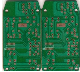
The mainstream PCB material classification mainly includes the following types: FR-4 (glass fiber cloth base), CEM-1/3 (glass fiber and paper composite substrate), FR-1 (paper-based copper clad laminate), metal-based laminate Copper plates (mainly aluminum-based, a few are iron-based) are currently more common types of materials, generally collectively referred to as rigid PCB.
The first three are generally suitable for products requiring high-performance electronic insulation, such as FPC reinforcement boards, PCB drilling pads, glass fiber mesons, potentiometer carbon film printed glass fiber boards, precision star gears (wafer grinding), and precision testing Sheets, electrical (electrical) equipment insulation stay spacers, insulation backing plates, transformer insulation plates, motor insulation parts, grinding gears, electronic switch insulation plates, etc.
The metal-based copper clad laminate is the basic material of the electronics industry, mainly used in the processing and manufacturing of printed circuit boards (PCB), which are widely used in electronic products such as televisions, radios, computers, computers, and mobile communications.
Extended information:

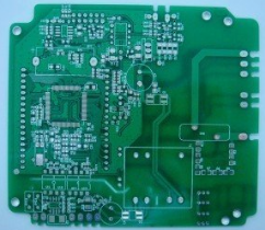
PCB (Printed Circuit Board), the Chinese name is printed circuit board, also known as printed circuit board, is an important electronic component, a support for electronic components, and a carrier for electrical connection of electronic components. Because it is made by electronic printing, it is called a "printed" circuit board.
After electronic equipment adopts printed boards, due to the consistency of similar printed boards, manual wiring errors can be avoided, and electronic components can be automatically inserted or mounted, automatic soldering, and automatic detection, ensuring the quality of electronic equipment, Improve labor productivity, reduce costs, and facilitate maintenance.
The reason why PCB can be used more and more widely is that it has many unique advantages, which are summarized as follows.
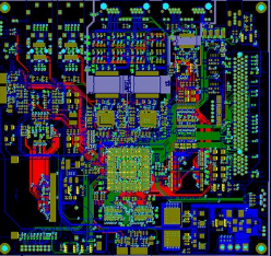
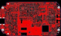
1 Can be high-density. For decades, the high density of printed boards has been able to develop along with the improvement of integrated circuit integration and the advancement of mounting technology.
2 High reliability. Through a series of inspections, tests and aging tests, the PCB can work reliably for a long time (usually 20 years).
3 Designability. For PCB performance (electrical, physical, chemical, mechanical, etc.) requirements, printed board design can be achieved through design standardization, standardization, etc., with short time and high efficiency.
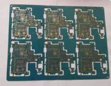
4 Manufacturability. With modern management, standardized, scaled (quantitative), automated and other production can be carried out to ensure product quality consistency.
5 Testability. A relatively complete test method, test standard, various test equipment and instruments have been established to detect and appraise the eligibility and service life of PCB products.
6 Can be assembled. PCB products are not only convenient for standardized assembly of various components, but also for automated and large-scale mass production. At the same time, PCB and various component assembly parts can be assembled to form larger parts and systems, up to the complete machine.
7 Maintainability. Since PCB products and various component assembly parts are designed and produced on a large scale, these parts are also standardized. Therefore, once the system fails, it can be replaced quickly, conveniently and flexibly, and the system can be quickly restored to work. Of course, there can be more examples. Such as miniaturization, light weight, high-speed signal transmission, etc.
Contact processing
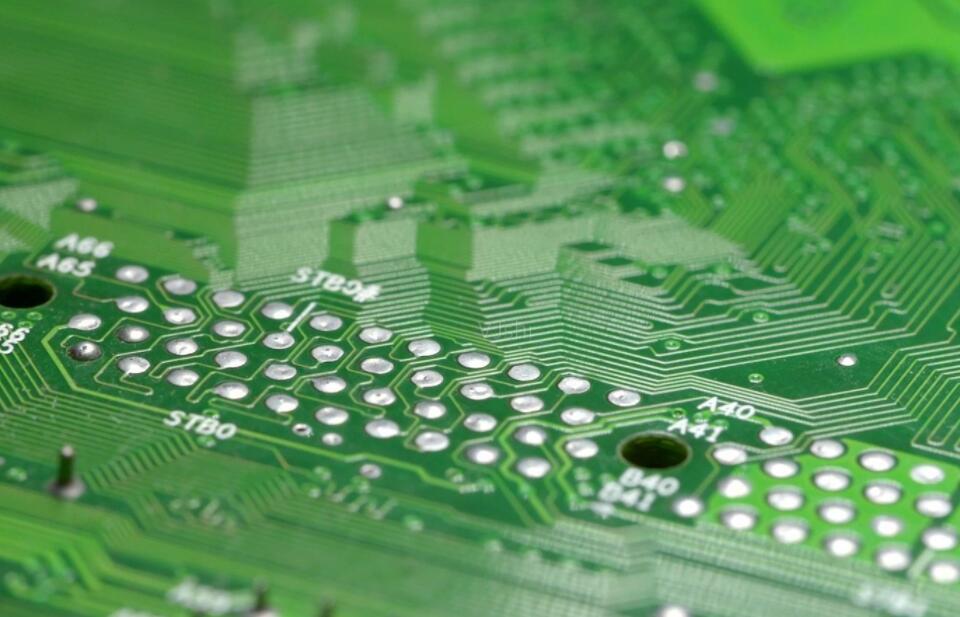
The solder resist green paint covers most of the copper surface of the circuit, only exposing the terminal contacts for part welding, electrical testing and circuit board insertion. This terminal needs to be added with a proper protective layer to avoid oxides generated at the terminal connected to the anode (+) during long-term use, which will affect the stability of the circuit and cause safety concerns.
【Plating hard gold】Plating a nickel layer and a highly chemically passivated gold layer on the socket terminals of the circuit board (commonly known as gold fingers) to protect the terminals and provide good connection performance. It contains a moderate amount of cobalt, which has excellent performance. The wear resistance characteristics.
[Snipping] The soldering end of the circuit board is covered with a layer of tin-lead alloy in a hot air leveling manner to protect the end of the circuit board and provide good soldering performance.
[Pre-solder] The soldering end of the circuit board is covered with a layer of anti-oxidation pre-soldering film by dip dyeing to temporarily protect the soldering end and provide a relatively flat soldering surface before welding, so that it has good soldering performance.
[Carbon ink] A layer of carbon ink is printed on the contact terminals of the circuit board by screen printing to protect the terminals and provide good connection performance.