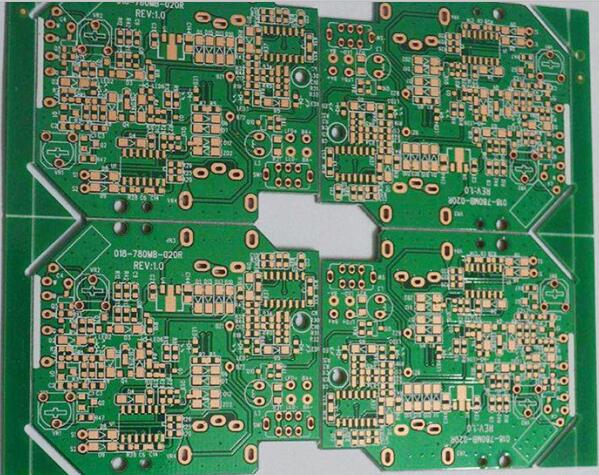
OSP is an organic solderability preservative (abbreviation for Organic Solderanility Preservative), this method is to complete the solder mask and characters on the printed circuit board, and perform OSP processing after electrical testing, and obtain the results in the exposed copper pads and through holes A heat-resistant organic solderable coating. The OSP process can replace the current hot air leveling (ie tin spraying) process, and the process is simple, fast, non-polluting, low in price, in line with EU standards, and gradually accepted by the electronics industry.

Circuit board osp introduction
OSP (Organic Solderability Preservatives), the Chinese translation is organic solder protection film, also known as copper protection agent and anti-oxidation. It is a kind of surface treatment performed in order to protect the copper surface of the solder joint with good soldering performance during the production process of the circuit board.
Simply put, OSP is to chemically grow a layer of organic film on the clean bare copper surface. This layer of film has anti-oxidation, thermal shock resistance, and moisture resistance to protect the copper surface from rusting (oxidation or sulfidation, etc.) in a normal environment; but in the subsequent welding high temperature, this kind of protective film must be very It is easy to be quickly removed by the flux, so that the exposed clean copper surface can be immediately combined with the molten solder into a strong solder joint in a very short time.
And there will be no residue. However, in the subsequent high temperature soldering, this protective film must be easily removed by the flux quickly, so that the exposed clean copper surface can be immediately combined with the molten solder into a strong solder joint in a very short time.
OSP process advantages
1. The process is simple and the amount of waste water is small
2. Smooth surface, good solderability
3, the operating temperature is low, no damage to the sheet
4, the cost is relatively low
OSP process disadvantages
1. Visual inspection is difficult and not suitable for multiple reflow soldering
2, OSP film surface is easy to scratch
3, high storage environment requirements
Limitations of the OSP process
1. Because OSP is transparent and colorless, it is difficult to check, and it is difficult to distinguish whether the PCB has been coated with OSP.
2, OSP itself is insulated, it does not conduct electricity. The OSP of Benzotriazoles is relatively thin and may not affect the electrical test, but for the OSP of Imidazoles, the protective film formed is relatively thick, which will affect the electrical test. OSP can't be used to handle electrical contact surfaces, such as keyboard surfaces for keys.
3. During the welding process of OSP, stronger Flux is needed, otherwise the protective film cannot be eliminated, which will lead to welding defects.
4. During the storage process, the surface of the OSP should not be exposed to acidic substances, and the temperature should not be too high, otherwise the OSP will volatilize.