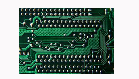
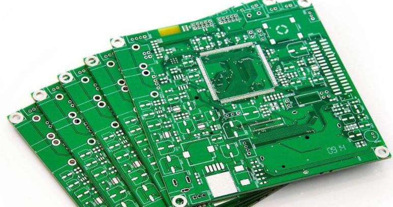
Some careful friends may find that there is a black thing on some circuit boards, so what is this kind of thing? In fact, this is a kind of package, we often call it "soft package", saying that it is actually a soft package For "hard", its constituent material is epoxy resin. We usually see that the receiving surface of the receiving head is also this material. Inside it is a chip IC. This process is called "bonding", and we usually Called "binding", let's talk about it in detail below.

Introduction to PCB Bonding
Bonding is a wire bonding method in the chip production process. It is generally used to connect the internal circuit of the chip with gold or aluminum wires to the package pins or the gold-plated copper foil of the circuit board before packaging. The ultrasonic waves from the ultrasonic generator (usually 40-140KHz), high-frequency vibration is generated by the transducer, and transmitted to the wedge through the horn, when the wedge is in contact with the lead wire and the welded part.
Under the action of pressure and vibration, the surface of the metal to be welded rubs against each other, the oxide film is destroyed, and plastic deformation occurs, causing the two pure metal surfaces to come into close contact, reaching the atomic distance combination, and finally forming a strong mechanical connection. Generally, after bonding (that is, after the circuit and the pins are connected), the chip is packaged with black glue.
Benefits of PCB Bonding
The advantage of the bonding packaging method is that the finished product is much higher than the traditional SMT patch method in terms of corrosion resistance, shock resistance and stability. At present, the most widely used SMT technology is to solder the pins of the chip on the circuit board. This production process is not suitable for the processing of mobile storage products. There are problems such as virtual soldering, false soldering, and missing soldering in the packaging test. .
In the course of daily use, the solder joints on the circuit board are exposed to the air for a long time and are affected by natural and man-made factors such as moisture, static electricity, physical wear, and acid corrosion, resulting in products prone to short circuit, open circuit, and even burnout.
The bonding chip connects the internal circuit of the chip with the circuit board package pins through gold wires, and then is covered with organic materials with special protection functions to complete the later package. The chip is completely protected by organic materials, isolated from the outside world, and does not exist. Occurrence of moisture, static electricity, and corrosion.
At the same time, the organic material melts at high temperature, is covered on the chip, and then dried by the instrument, seamlessly connected to the chip, completely preventing the physical wear of the chip, and has higher stability.
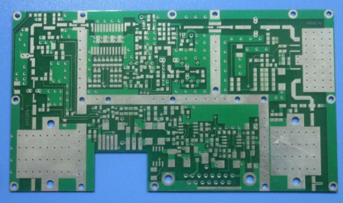
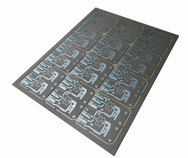
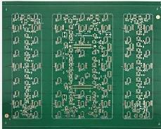
Multilayer circuit board introduction
Multi-layer circuit board is a multilayer wiring layer, and there is a dielectric layer between every two layers, and the dielectric layer can be made very thin.Multilayer circuit boards have at least three conductive layers, two of which are on the outer surface, and the remaining layer is integrated into the insulating board. The electrical connection between them is usually achieved through plated through holes on the cross section of the circuit board.
It was first called "Build Up Multilayer PCB" in Japan. It is on an insulating substrate, or on a traditional double-sided or multi-layered board, which is coated with an insulating medium and then electroless copper plating It forms wires and connection holes with electroplated copper, and superimposes so many times to form a multi-layer printed board with the required number of layers.