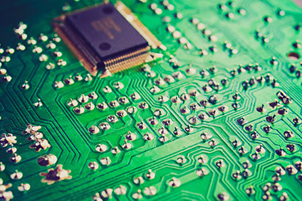
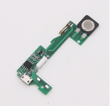
Talk about PCB assembly solderless press-in connection technology and material problems
Before sharing this topic, Baiqiancheng will first talk about what solderless press-in connection technology is. The PCB assembly solderless press-in connection technology, also known as crimping technology, is a kind of "moderate compression" established by the elastic deformable connector or the rigid connector embedded in the metalized holes of two or more layers of printed boards. In” connection, a close contact surface is established between the terminal and the metalized hole, and the electrical connection is completed by mechanical connection.
The crimping technology has high safety and reliability, plug-in safety performance and easy maneuverability, which prevents the problem of excessive heat absorption during reflow soldering, and it is not easy to cause the plug of the connector to be damaged or cracked; At the same time, there is no need for solder and flux, which solves the problems of difficult cleaning of the welded parts and easy oxidation of the welded surface. For this reason, the crimping technology has been extended to the present and is still widely accepted and applied.
The main factors of PCB assembly crimping technology:
1. Press-in terminal; 2. Printed board; 3. Crimp processing technology; 4. Special tools and equipment for crimping
1. Press-in connection

Press-in terminals (crimped pins) are divided into rigid pins and flexible pins (as shown in the figure). The rigid pin does not cause deformation during the crimping process, but the hole will deform:
PCB rigidity and flexibility
The flexible pin will be squeezed and deformed during the crimping process, but the hole will not be deformed
(1) Material
The crimping should use a more suitable grade of copper alloy. Such as copper tin alloy, bronze copper zinc alloy, brass or beryllium copper alloy.
The selection of materials not only depends on the size and function of the parts, but also must be consistent with the requirements of the electrical connection with excellent stability.
All materials are related to time, temperature and stress, leading to stress relaxation.
The terminal material and structure are such that when the force to maintain the connection is not easy to reduce, the resistance at the connection point increases to an unacceptable level.
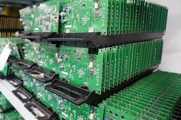
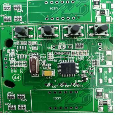
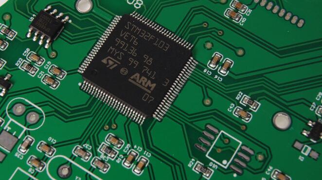
A whole PCB assembly process is an intricate and complicated process that requires overall details to be controlled. For SMT
All product quality problems of patch and even PCB light board circuit boards will lead to product defects.
At present, the country has higher and higher requirements for environmental protection and greater efforts in link governance. This is a challenge but also an opportunity for PCB factories. If PCB factories are determined to solve the problem of environmental pollution, then FPC flexible circuit board products can be at the forefront of the market, and PCB factories can get opportunities for further development.
The Internet era has broken the traditional marketing model, and a large number of resources have been gathered together to the greatest extent through the Internet, which has also accelerated the development speed of FPC flexible circuit boards, and then as the development speed accelerates, environmental problems will continue to appear in PCB factories. In front of him. However, with the development of the Internet, environmental protection and environmental informatization have also been developed by leaps and bounds. Environmental information data centers and green electronic procurement are gradually being applied to the actual production and operation fields. From this point of view, the environmental protection problems of PCB factories can be solved from the following two points.