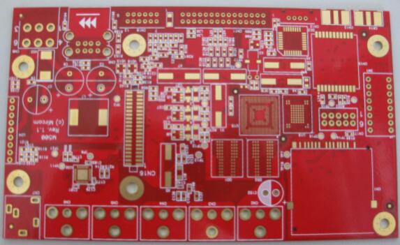
A brief introduction to the electrical reliability of PCB assembly manufacturing
Hello everyone, what I shared today is PCB assembly manufacturing electrical reliability, soldering, wave soldering, repairing and other processes, which may form different residues. In a humid environment and a certain voltage, an electrochemical reaction may occur between the same PCB circuit board and the conductor, resulting in a decrease in surface insulation resistance (SIR). If electromigration and dendrite growth occur, there will be a short circuit between the wires, resulting in a risk of electromigration (commonly known as "leakage").
A brief introduction to the electrical reliability of PCB assembly manufacturing
In order to ensure electrical reliability, it is necessary to evaluate the performance of different non-cleaning agents, try to use the same flux for the same PCB, or perform post-weld cleaning treatment.

According to the reliability analysis of the solder joints in seven aspects: mechanical strength, tin whiskers, voids, cracks, intermetallic compound cellularity, mechanical vibration failure, thermal cycle failure and electrical reliability, in the solder joints with the following defects, Any kind of failure is more likely to occur: the thickness of the intermetallic compound after welding is too thin or too thick: there are holes and micro cracks in the solder joint or interface; the wetted area of the solder joint is small (the size of the joint between the solder end of the component and the pad is small): The solder joint structure is not dense, the crystal particles are large, and the internal stress is large.
Some defects can be detected by visual inspection, AOI and X-ray, such as small overlap size of solder joints, pores on the surface of solder joints, obvious cracks, etc. However, the microstructure, internal stress, internal voids and cracks of the solder joints, especially the thickness of intermetallic compounds, these hidden defects are invisible to the naked eye and cannot be detected by manual or automatic SMT processing. A variety of reliability tests and analysis are used for testing, such as temperature cycling, vibration test, drop test, high temperature storage test, damp heat test, electromigration (ECM) test, highly accelerated life test and highly accelerated stress screening; then test solder joints The electrical and mechanical properties (such as the shear strength and tensile strength of solder joints); finally can be judged by visual inspection, X-ray fluoroscopy, metallographic section, scanning electron microscope and other test analysis.
It can also be seen from the above analysis that hidden defects add uncertain factors to the long-term reliability of lead-free products. Therefore, current high-reliability products have been exempted; whether it is obvious or hidden defects, it is caused by factors such as lead-free high tin, high temperature, small process window, poor wettability, material compatibility, design, process and management. Caused.
Therefore, we must start with the design of PCB assembly lead-free products to consider the compatibility between lead-free materials, the compatibility between lead-free and design, and the compatibility between lead-free and process; and fully consider the heat dissipation problem and carefully choose PCB Board, pad surface, components, solder paste and flux, etc.; SMT process optimization and process control are more detailed than lead soldering, and material management is carried out more strictly and meticulously.