Analysis on the related problems of solder point sharpening in PCB assembly welding
Many customers will ask about the problem of PCB assembly processing through rate. In fact, PCB assembly processing through rate refers to how much time it takes for the product to go from the previous process to the next process. The less time, the higher the efficiency, the better the quality. Because you can proceed to the next step only when there is no problem with your product. With the problem of through rate of PCB assembly processing, today's electronic editor will share the related problems of soldering point sharpening in PCB assembly welding.
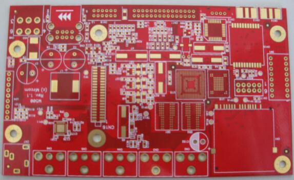
PCB solder joints
1. In the preheating stage, the temperature of the PCB circuit board is too low and the preheating time is too short, which makes the temperature of the PCB and the components low, and the components and the PCB absorb heat during soldering to produce a convex tendency.
2. The temperature of SMT chip soldering is too low or the conveyor speed is too fast, so that the viscosity of the molten solder is too large.
3. The wave crest height of the electromagnetic pump wave soldering machine is too high or the pin is too long, so that the bottom of the pin cannot touch the wave crest. Because the electromagnetic pump wave soldering machine is a hollow wave, the thickness of the hollow wave is 4~5mm.
4. Poor flux activity.
5. The ratio of the lead diameter of the DIP plug-in component to the plug-in hole is incorrect, the plug-in hole is too large, and the large pad absorbs a large amount of heat.

The above problems are the most important factors that cause the solder joints to sharpen, so we should make corresponding optimizations and adjustments to the above problems in the smt patch processing, solve the problems before they occur, and ensure the yield and delivery speed of the products. .
1. The tin wave temperature is 250 degree Celsius±5 degree Celsius, and the welding time is 3~5s; when the temperature is slightly lower, the speed of the conveyor belt will be slower.
2. The height of the wave crest is generally controlled at 2/3 of the thickness of the printed board. The pin forming of the interposing component requires the component pin to be exposed and printed
3. The welding surface of the board is 0.8mm~3mm.
4. Replace the flux.
5. The aperture of the insertion hole is 0.15~0.4mm larger than the diameter of the lead wire (the thin lead wire is removed, and the thick lead wire is the upper limit).
The above is about the generation and solution of solder joints in PCB assembly welding. I hope to help everyone.
help. Simply analyze the related problems of solder joint tipping in PCB assembly welding and share it here. Please continue to pay attention to learn more about PCB assembly.
Our factory is located in China. For decades, Shenzhen has been known as the world's electronics R&D and manufacturing center. Our factory and website are approved by the Chinese government, so you can skip the middleman and buy products on our website with confidence. Because we are a direct factory, this is the reason why 100% of our old customers continue to purchase on iPCB.
No minimum requirements
You can order as little as 1 PCB from us. We will not force you to buy things you really don't need to save money.
Free DFM
Before you pay in the most timely manner, all your orders will receive free engineering document review services by our well-trained professional and technical personnel.