1 Introduction
With the development of science and technology, especially the advancement in the materials of integrated circuits, the computing speed has been significantly improved, and the integrated circuits are driven to high density, small size, and single parts. All of these have led to the high frequency response of today's and future printed circuit boards. The use of high-speed digital circuits means that the impedance of the line must be controlled, low distortion, low interference and low crosstalk, and the elimination of electromagnetic interference EMI. Impedance design is becoming more and more important in PCB design. As the front part of the PCB manufacturing front-end, it is responsible for the simulation calculation of impedance and the design of the impedance bar. Customers have become more and more demanding on impedance control, and the number of impedance controls has increased. How to quickly and accurately design impedance is a problem that the pre-system personnel are very concerned about.
2. Main types of impedance and influencing factors
Impedance (Zo) definition: The total resistance to alternating current flowing through it at a known frequency is called impedance (Zo). For printed circuit boards, it refers to the total impedance of a certain circuit layer (signal layer) to its closest reference plane under high-frequency signals.
2.1 Impedance type:
(1) Characteristic impedance. In electronic information products such as computers and wireless communications, the energy transmitted in the PCB circuit is a square wave signal (called pulse) composed of voltage and time. The resistance encountered is called the characteristic impedance.
(2) Differential Impedance” Two identical signal waveforms with opposite polarities are input at the drive end, which are respectively transmitted by two differential lines, and the two differential signals are subtracted at the receiving end. The differential impedance is the impedance Zdiff between the two wires.
(3) Odd Mode Impedance The impedance value of one line to the ground of the two lines is the same as the impedance value of the two lines.
(4) Even Mode Impedance Two same signal waveforms with the same polarity are input at the drive end, and the impedance Zcom when the two wires are connected together.

(5) Common Mode Impedance The impedance Zoe of one of the two wires to the ground, the impedance value of the two wires is the same, usually larger than the odd mode impedance.
Among them, characteristic and differential are common impedances, and common mode and odd mode are rare.
2.2 Factors affecting impedance:
W-----line width/line-to-line the line width increases and the impedance decreases, and the distance increases the impedance increases;
H----Insulation thickness The thickness increases and the impedance increases;
T------copper thickness copper thickness increases and impedance decreases;
H1---green oil thick the thickness increases and the impedance decreases;
Er-----Dielectric constant reference layer DK value increases, impedance decreases;
Undercut----W1-W undercut increases, the impedance becomes larger.
3, impedance calculation automation
Si8000 is a new boundary element method field effect solution calculator software, based on the easy-to-use user interface of the early Polar impedance design system we are familiar with. This software contains various impedance modules. The personnel can calculate impedance results by selecting specific modules, inputting line width, line spacing, interlayer thickness, copper thickness, Er value and other related data. A PCB impedance control number can be as few as 4 or 5 groups, and as many as dozens of groups. Each group has different control line width, interlayer thickness, copper thickness, etc. If you check the data one by one, then manually enter the relevant parameter calculations, Very time-consuming and error-prone.
4, automatically generate impedance bar
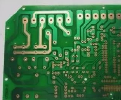
If the customer does not design the impedance bar by ourselves, we need to design the impedance bar by ourselves and put it on the edge of the board or the broken edge (generally, the impedance bar is placed on the broken edge and requires the customer's consent). The circuit board manufacturer designs an impedance bar on the side of the circuit board that meets all the characteristics and parameters of the customer's impedance control. By testing the impedance value of the impedance bar, it reflects that the circuit board meets the customer's impedance control requirements. To correctly test the impedance value in the board, the key lies in the design of the impedance bar.
The general PCB factory impedance bar design method is: MI engineers fill in the impedance attachment form according to the calculated impedance result, such as impedance value, reference layer, control line width, test hole, reference layer attribute (positive and negative film), etc.
Then, the CAM engineer manually makes the impedance bar according to the impedance table provided by MI, or enters the relevant impedance data through Script, and runs the impedance bar with the program. Under normal circumstances, we design an impedance bar for one impedance value, and it usually takes about 10 minutes to make an impedance bar. Repeated manual data filling is very time-consuming and error-prone.
InCoupon adopts an embedded development architecture, which can detect the ideal drilling position between the layers at the level of the semi-finished product, so that the drilling operations of the existing plate layers can be completely consistent with the Coupon circuit layers, and a complete CAM is integrated. Coupon circuit, development structure and semi-finished product table for impedance measurement are produced with engineering technology, and the optimal interconnection ability can be found for the coupon level, and the complex and manual calculation can be replaced by intelligent operation wizard, which can be automatically in a few seconds. Calculate the reliable measurement circuit Coupon, making the design of the Coupon a simple and standard task.
5. Summary
PCB competition is becoming more and more fierce, the sample delivery time is getting shorter and shorter, and impedance design accounts for a large proportion of the pre-production work. How to shorten the impedance production time and make impedance matching that meets customer requirements is a must A question to consider. The appearance of InPlan and InCoupon has provided very good help to impedance design. Of course, each PCB board manufacturer's own impedance calculation rules, Layout method and size will be different. InPlan system needs special personnel to develop and maintain, in order to truly realize its functions. But I believe that the automation of impedance design will become more and more popular in the front omanufacturing.