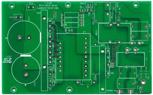
With the increasing popularity of plasma processing technology, there are currently the following functions in the PCB manufacturing process:
(1) Hole wall erosion / Removal of resin drilling dirt on the hole wall
For general FR-4 multilayer printed circuit board manufacturing, the removal of resin drilling and etch treatment after numerical control drilling usually includes concentrated sulfuric acid treatment, chromic acid treatment, and alkaline potassium permanganate. Solution treatment method and plasma treatment method.
However, for flexible printed circuit boards and rigid-flexible printed circuit boards to remove drilling stains, due to the different characteristics of the materials, if the above-mentioned chemical treatment is used, the effect is not ideal, and plasma is used to remove Drilling dirt and etchback can obtain better roughness of the hole wall, which is beneficial to hole metallization and electroplating, and at the same time has the "three-dimensional" etchback connection characteristics.
(2) Activation treatment of polytetrafluoroethylene material
However, all engineers who have conducted hole metallization of PTFE materials have this experience: using general FR-4 multilayer printed circuit board hole metallization methods, it is impossible to obtain PTFE with successful hole metallization. Vinyl printed circuit board. The biggest difficulty is the pretreatment of PTFE activation before electroless copper deposition, which is also the most critical step.
There are a variety of methods for the activation treatment before electroless copper deposition of PTFE materials, but in summary, to ensure product quality and suitable for batch production, there are mainly the following two methods:

(A) Chemical treatment method
"Metal sodium and naphthalene react in a solution of non-aqueous solvents such as tetrahydrofuran or ethylene glycol dimethyl ether to form a sodium naphthalene complex. The sodium naphthalene treatment solution can make the polytetrafluoroethylene surface layer atoms in the hole be etched, so as to achieve the purpose of wetting the hole wall. This is a classic and successful method with good results and stable quality. It is currently the most widely used.
(B) Plasma treatment method
This processing method is a dry process, which is easy to operate, stable and reliable in processing quality, and is suitable for mass production. As for the sodium naphthalene treatment liquid of the chemical treatment method, it is difficult to synthesize, has high toxicity, and has a short shelf life. It needs to be formulated according to the production situation and has high safety requirements.
Therefore, at present, most of the activation treatment of the polytetrafluoroethylene surface is carried out by plasma treatment, which is convenient to operate and significantly reduces waste water treatment.
(3) Carbide removal
Plasma treatment method not only has obvious effects in the drilling and dirt treatment of all kinds of sheets, but also shows its superiority in removing the drilling dirt of composite resin materials and micro-holes. In addition, with the increasing demand for higher interconnect density laminated multilayer printed circuit board manufacturing, a large number of laser technology is used to drill blind hole manufacturing, as a by-product of laser drilling blind hole application-carbon In other words, it needs to be removed before the hole metallization process. At this time, the plasma treatment technology, without any denial, has taken on the important task of removing carbides.
(4) Inner pretreatment
With the increasing demand for various types of printed circuit board manufacturing, higher and higher requirements are put forward for the corresponding processing technology. Among them, the inner layer pretreatment of flexible printed circuit boards and rigid-flexible printed circuit boards can increase the surface roughness and activity, and improve the bonding force between the inner layers of the board, which is also critical for successful manufacturing. .
In this regard, plasma processing technology has shown its unique charm, and there are many successful examples. In addition, before the solder mask is coated, plasma is used to treat the printed circuit board surface to obtain a certain degree of roughness and a highly active surface, thereby improving the adhesion of the solder mask.
(5) Residue removal
Plasma technology has the following three functions in the removal of residues:
(A) In the manufacture of printed circuit boards, especially in the production of fine lines, plasma is used to remove dry film residues/residual glue before etching to obtain perfect and high-quality wire patterns. If, once after development and before etching, the resist is not cleanly removed, it will cause the occurrence of short circuit defects.
(B) Plasma treatment technology can also be used to remove residual solder mask and improve solderability.
(C) For some special plates, when electroplating solderable coatings after pattern etching is used, due to the presence of copper particles that are not cleanly etched on the edge of the circuit, shadow plating will occur, and the product will be scrapped in severe cases. At this time, plasma treatment technology can be used to remove the fine copper particles through ablation, and finally realize the processing of qualified products.
Therefore, the PCB factory should pay attention to the plasma surface pretreatment in the PCB board manufacturing process.