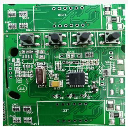
What are the common surface treatment methods for PCB circuit boards
1. Hot air leveling
The process of coating molten tin-lead solder on the surface of the PCB and flattening (flattening) with heated compressed air makes it form a coating layer that is resistant to copper oxidation and provides good solderability. During hot air leveling, the solder and copper form a copper-tin metal compound at the junction, and the thickness is about 1 to 2 mils;
2. Electroless nickel gold
A thick layer of nickel-gold alloy with good electrical properties is wrapped on the copper surface and can protect the PCB for a long time. Unlike OSP, which is only used as an anti-rust barrier layer, it can be useful in the long-term use of PCB and achieve good electrical performance. In addition, it also has tolerance to the environment that other surface treatment processes do not have;
3. Organic anti-oxidation
On the clean bare copper surface, an organic film is grown chemically. This layer of film has anti-oxidation, heat shock resistance, and moisture resistance to protect the copper surface from rusting (oxidation or sulfidation, etc.) in a normal environment; at the same time, it must be easily assisted in the subsequent welding high temperature The flux is quickly removed to facilitate welding;

PCB circuit board manufacturers
4. Chemical Immersion Silver
Between OSP and electroless nickel/immersion gold, the process is simpler and faster. When exposed to heat, humidity and pollution, it can still provide good electrical performance and maintain good solderability, but it will lose its luster. Because there is no nickel under the silver layer, immersion silver does not have the good physical strength of electroless nickel/immersion gold;
5. Electroplated nickel gold
The conductor on the PCB surface is electroplated with a layer of nickel and then electroplated with a layer of gold. The main purpose of nickel plating is to prevent the diffusion between gold and copper. There are two types of electroplated nickel gold: soft gold plating (pure gold, gold indicates that it does not look bright) and hard gold plating (the surface is smooth and hard, wear-resistant, contains cobalt and other elements, and the surface looks brighter). Soft gold is mainly used for gold wire during chip packaging; hard gold is mainly used for electrical interconnection in non-soldering places (such as gold fingers).
6. PCB hybrid surface treatment technology
Choose two or more surface treatment methods for surface treatment. The common forms are: Immersion Nickel Gold + Anti-oxidation, Electroplating Nickel Gold + Immersion Nickel Gold, Electroplating Nickel Gold + Hot Air Leveling, Immersion Nickel Gold + Hot Air Leveling . Among all surface treatment methods, hot air leveling (lead-free/leaded) is the most common and cheaper treatment method, but please pay attention to the EU's RoHS regulations.
7. Random characters
The SMD soldering pad of the character cover pad brings inconvenience to the continuity test of the printed board and the soldering of the components. The character design is too small, making screen printing difficult, and too large will cause the characters to overlap each other and make it difficult to distinguish
8. Single-sided pad aperture setting
Single-sided pads of circuit boards are generally not drilled. If the drilled holes need to be marked, the hole diameter should be designed to be zero. If the value is designed, then when the drilling data is generated, the hole coordinates will appear at this position, and there will be a problem. Single-sided pads such as drilling should be specially marked.