Flexible ted Circuit (FPC Flexible Printed Circuit) is a form of circuit fabricated on a flexible cut-off surface, which may or may not have a cover layer (usually used to protect the FPC circuit). Since FPC can be bent, folded or repetitively moved in a variety of ways, compared with ordinary rigid boards (PCB), it has the advantages of lightness, thinness, flexibility, etc, so its application is more and more extensive.
FPC base film (Base Film) material generally uses polyimide (Polyimide, PI for short), but also polyester
(Polyester, referred to as PET), the material thickness is 12.5/25/50/75/125um, commonly used 12.5 and 25um. If FPC needs to be welded at high temperature, PI is usually selected as the material, and FR4 is usually selected as the base material of PCB.
The cover layer of FPC is made of a laminated body of dielectric film and glue, or a coating of flexible medium, which has the protective effect of avoiding contamination, moisture, scratches, etc. The main material is the same as that of the base layer, namely polyimide amine
(Polyimide) and polyester (Polyester), the thickness of commonly used materials is 12.5um.

FPC design needs to bond each layer together, this time you need to use FPC glue (Adhesive). Commonly used adhesives for flexible boards include Acrylic, Modified Epoxy, Phenolic Butyrals, Reinforced Adhesives, Pressure Sensitive Adhesives, etc., while single-layer FPC does not need to use glue for bonding.
In many applications such as device welding, the flexible board needs to use a stiffener to obtain external support. The main materials used are PI or Polyester film, glass fiber, polymer material, steel sheet, aluminum sheet and so on. PI or Polyester film is a commonly used material for the reinforcement of flexible boards, and the thickness is generally 125um. The hardness of the glass fiber (FR4) reinforcement board is higher than that of PI or Polyester, and it is relatively difficult to process when it is used in places where it is required to be harder.
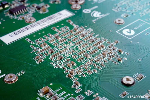
Compared with the PCB pad processing method, FPC pad processing also has a variety of methods, the common ones are as follows:
1. Chemical nickel gold is also called chemical immersion gold or immersion gold. Generally, the thickness of the electroless nickel layer used on the copper metal surface of the PCB is 2.5um-5.0um, and the thickness of the immersion gold (99.9% pure gold) layer is 0.05um-0.1um. Replace the gold in the PCB pool). The technical advantages: flat surface, longer storage time, easy to solder; suitable for fine-pitch components and thinner PCBs. For FPC, it is more suitable because of its thinner thickness. Disadvantages: not environmentally friendly.
2. The advantages of Tin-Lead Plating: You can directly add flat lead and tin to the pad, with good solderability and uniformity. For some processing techniques such as HOTBAR, this method must be adopted on FPC. Disadvantages: lead is easy to oxidize, and the storage time is short; it needs to pull the electroplated wire; it is not environmentally friendly.
3. Selective gold electroplating (SEG) Selective gold electroplating refers to the use of electroplated gold in local areas of the PCB, and another surface treatment method for other areas. Gold electroplating refers to coating the copper surface of the PCB with a nickel layer first, and then electroplating the gold layer. The thickness of the nickel layer is 2.5um-5.0um, and the thickness of the gold layer is generally 0.05um-0.1um. Advantages: thick gold plating, strong oxidation resistance and wear resistance. "Golden Finger" generally adopts this processing method. Disadvantages: not environmentally friendly, cyanide pollution.
4. Organic Solderability Protective Layer (OSP) This process refers to covering the exposed PCB copper surface with specific organic matter. Advantages: It can provide a very flat PCB surface, which meets environmental protection requirements. Suitable for PCBs with fine pitch components.
Disadvantages:PCBA using conventional wave soldering and selective wave soldering processes is required, and OSP surface treatment processes are not allowed.
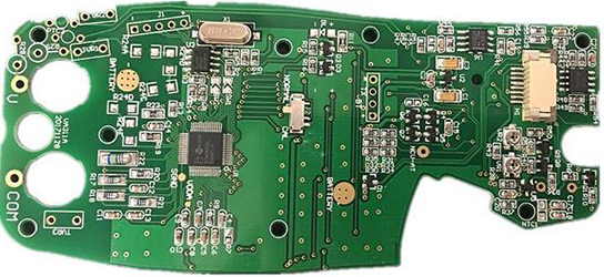
In the design, FPC often needs to be used in conjunction with PCB. In the connection between the two, board-to-board connectors, connectors with gold fingers, HOTBAR, soft and hard boards, and manual soldering are usually used for connection. For different applications Environment, the designer can adopt the corresponding connection method.
In actual applications, it is necessary to determine whether ESD shielding is required according to the application needs. When the FPC flexibility requirements are not high, it can be realized with solid copper and thick media. When the flexibility requirements are high, it can be realized by using copper skin grid and conductive silver paste.
Due to the flexibility of FPC, it is easy to break when subjected to stress, so some special measures are required for FPC protection.
The commonly used methods are:
1. The minimum radius of the inner corner on the flexible contour is 1.6mm. The larger the radius, the higher the reliability and the stronger the tear resistance. At the corner of the shape, a trace near the edge of the board can be added to prevent the FPC from being torn.
2. The crack or slot on the FPC must end in a round hole with a diameter of not less than 1.5mm. This is also required when the two adjacent parts of the FPC need to be moved separately.
3. In order to achieve better flexibility, the bending area needs to be selected in a uniform width area, and try to avoid the FPC width change and uneven wiring density in the bending area.
4. Stiffener, also known as stiffener, is mainly used to obtain external support. The materials used are PI, Polyester, glass fiber, polymer materials, aluminum sheets, steel sheets, etc. Reasonable design of the position, area and material of the reinforcing plate has a great effect on avoiding FPC tearing.
5. In the multi-layer FPC design, the area that needs to be bent frequently during the use of the product needs to be designed with air gap layers. Try to use thin PI materials to increase the softness of the FPC and prevent the FPC from breaking during repeated bending.
6. When space permits, a double-sided tape fixing area should be designed at the junction of the golden finger and the connector to prevent the golden finger and the connector from falling off during the bending process.
7. The FPC positioning silk screen line should be designed at the connection between the FPC and the connector to prevent the FPC from skewing and improper insertion during the assembly process. Conducive to production inspections.
Due to the particularity of FPC, the following points need to be paid attention to when wiring:
Wiring rules: Give priority to ensuring smooth signal wiring, follow the principle of short, straight, and less perforation, try to avoid long, thin and circular wiring, mainly horizontal, vertical and 45-degree lines, avoid random The angle line and the curved part follow the arc line. The above conditions are described in detail as follows:
1. Line width: Considering that the line width requirements of the data line and the power line are inconsistent, the reserved wiring space is 0.15mm on average
2. Line pitch: According to the current production capacity of most manufacturers, the design line pitch (Pitch) is 0.10mm
3. Line margin: The distance between the outermost line and the FPC contour is designed to be 0.30mm, and the larger the space is, the better
4. Internal fillet: The minimum internal fillet on the FPC profile is designed to be radius R=1.5mm
5. The wire is perpendicular to the bending direction
6. The wire should pass through the bending area evenly
7. The wire shall be as full as possible in the area of the bending area
With the expansion of the FPC application environment, the above content will continue to be enriched or not applicable, but as long as you design carefully in your work, think more and summarize, I believe that designing an FPC is not difficult, and you can easily get started.