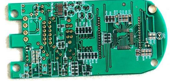
Hello everyone, I am the editor, today I will talk to you about the anti-jamming design principles of printed PCB circuit boards, let’s take a look at it together.
1. Power cord layout:
1. According to the current size, try to widen the wire wiring.
2. The direction of the power cord and ground wire should be consistent with the direction of data transmission.
3. A decoupling capacitor of 10~100μF should be connected to the power input end of the printed board.
Two ground wire layout:
1. The digital ground is separated from the analog ground.
2. The grounding wire should be as thick as possible, so that it can pass 3 times the allowable current on the printed board, and generally should be 2~3mm.3. The grounding wire should form an endless loop as far as possible, so as to reduce the potential difference of the grounding wire.

Eight layers of green oil lead-free tin plate
Three decoupling capacitor configuration:
1. Connect a 10~100μF electrolytic capacitor across the power input end of the printed board, if it can be greater than 100μF, it is better.
2. Connect a 0.01~0.1μF ceramic capacitor between Vcc and GND of each integrated chip. If space is not allowed, a 1~10μF tantalum capacitor can be configured for every 4~10 chips.
3. Devices with weak anti-noise ability and large change in turn-off current, as well as ROM and RAM, should indirectly decoupling capacitors between Vcc and GND.
4. Match a 0.01μF decoupling capacitor on the reset terminal "RESET" of the microcontroller.
5. The leads of decoupling capacitors should not be too long, especially high-frequency bypass capacitors.
Four device configuration:
1. The clock input terminals of the clock generator, crystal oscillator and CPU should be as close as possible and far away from other low-frequency devices.
2. Keep small current circuits and high current circuits away from logic circuits as much as possible.
3. The position and direction of the printed board in the chassis should ensure that the device with a large amount of heat is on the top.
Five power lines, AC lines and signal lines are routed separately
The power line and AC line should be placed on a different board from the signal line as much as possible, otherwise they should be routed separately from the signal line.
Six other principles:
1. Add a pull-up resistor of about 10K to the bus, which is conducive to anti-interference.
2. When wiring, the address lines should be as long as possible and as short as possible.
3. The lines on both sides of the PCB should be arranged vertically as far as possible to prevent mutual interference.
4. The size of the decoupling capacitor is generally C=1/F, and F is the data transmission frequency.
5. Unused pins are connected to Vcc through a pull-up resistor (about 10K), or connected in parallel with the used pins.
6. Heat-generating components (such as high-power resistors, etc.) should avoid components that are easily affected by temperature (such as electrolytic capacitors, etc.).
7. The use of full decoding has stronger anti-jamming performance than line decoding.