Take ESD as an example
Signal current in layer conversion
Abstract: Printed circuit boards, PCBs, and signal paths must often change the layers in the board stack. In some cases, this can cause problems. ESD examples are used to illustrate the conditions under which changing layers can cause problems.
Signal path through via
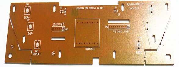
Discussion: The routing path in the PCB usually requires changing the path of the layers to complete the layout. For a four-layer PCB, this usually means changing from the top layer of the circuit board to the bottom layer, and the two middle layers are power and ground. Four-layer boards are particularly problematic because the separation between the power and ground planes is usually relatively large compared to six or more layers, about 30 to 40 mils.
On the top and bottom layers, the signal current matches its mirrored return current in the nearby ground or power plane. As the signal current changes layers from top to bottom, damage that affects ESD performance may occur.

All signals form a loop, from source to loading, and back to the source. It is usually the "return" part of the path that gets us into trouble, as we will see in this particular case. The return current of the signal at the bottom of the bottom surface follows the signal to the top of the bottom surface, but it must pass through the inter-surface impedance to reach the bottom of the top surface, from where it can follow the signal to the top of the top surface.
Test board with single-layer and two-layer paths
One way to consider impedance Z is to think of the two planes as a two-dimensional transmission line extending from the signal via. Bypass capacitors form low impedance "short circuits" (although short circuits are not so good at high enough frequencies because their inductance becomes important) and the edges of the circuit board are usually unterminated "open circuits". These and other features can cause reflections, causing the impedance between the planes to vary significantly with frequency, and for a four-layer board with a plane spacing of about 30 mils, it can reach several ohms at certain frequencies. Murphy's law states that a peak of this impedance will be at the third harmonic of the clock frequency!
To evaluate this effect, I built a test board as shown in Figure 2. Each signal trace is about 30 cm long. The wiring consists of a 100-ohm twisted-pair telephone wire conductor. When attached to the ground plane, it forms a 50 ohm path. The board is a double copper clad laminate, and the entire assembly simulates a four-layer PWB. The two copper planes are about 30 mils apart and are shorted together via the SMA connector on the left and the load resistor (four positions) on the right. One path stays on one side, while the other path penetrates the circuit board and runs about 10 cm on the other side.
Test board with single-layer and two-layer paths
The circuit board is subjected to 3 kV ESD contact discharge, from the ESD simulator to the end of a 1 meter cable, which is fixed on the plane shown in Figure 2 near the middle of the right edge, and the middle of the left edge is connected to the ground to discharge the charge from the board .
EMI generated by ESD to the first layer path
For example, the apparent signal at the SMA connector of the path below, the signal changes layers from the top to the bottom of the circuit board and then back. In this case, the peak signal at the SMA connector exceeds the 2 volt peak and oscillates at the natural frequency of the component. For most logic circuits, this level is definitely a problem. The increased noise in the lower path is due to the voltage drop across the board impedance Z caused by ESD at each transition from one side of the board to the other. This voltage appears in the signal/return circuit and therefore appears on the SMA connector.
Signal at SMA connector
EMI generated by ESD to the two-layer path
For the case where the distance between the boards is much less than 30 mils, the impedance between the boards will usually be lower, and the effect shown in Figure 4 will be smaller and there will be fewer problems. If the critical signal transitions from the top of the circuit board close to the existing (low-cost) bypass capacitor to the bottom, the impact on the four-layer circuit board can also be minimized.
Summary: The conversion between PWB layers can cause significant damage to the signal path. The greater the distance between the power supply and the ground plane, the greater the impact. An example of a "four-layer" PWB responding to ESD shows one of the possible problems.