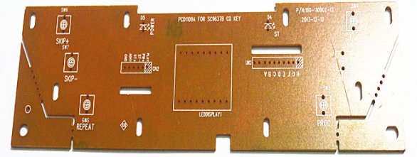
In the PCB circuit board production, the reflow furnace is prone to board bending and board warping, so how to prevent the PCB circuit board from going through the reflow furnace from board bending and board warping, the following is a detailed explanation for everyone:
1. Reduce the influence of temperature on PCB circuit board stress
Since "temperature" is the main source of circuit board stress, as long as the temperature of the reflow furnace is reduced or the rate of heating and cooling of the circuit board production in the reflow furnace is slowed, the bending and warpage of the board can be greatly reduced. happen. However, other side effects may occur, such as solder short circuit.
2.PCB with high Tg board
Tg is the glass transition temperature, that is, the temperature at which the material changes from the glass state to the rubber state. The lower the Tg value of the material, the faster the circuit board starts to soften after entering the reflow furnace, and it becomes soft rubber state The time will also be longer, and the deformation of the circuit board will of course be more serious. The use of a higher Tg board can increase its ability to withstand stress and deformation, but the price of the relatively high material for the production of circuit boards is also relatively high.

3. Increase the thickness of the PCB circuit board
In order to achieve the purpose of lighter and thinner for many electronic products, the thickness of the circuit board has been left 1.0mm, 0.8mm, and even 0.6mm thickness. This thickness must keep the circuit board from deforming after the reflow furnace, which is really a bit It is difficult for others. It is recommended that if there is no requirement for lightness and thinness, the circuit board can be used with a thickness of 1.6mm, which can greatly reduce the risk of bending and deformation of the board.
4. Reduce the size of the circuit board and reduce the number of puzzles
Since most of the reflow furnaces use chains to drive the circuit board forward, the larger the PCB design size, the circuit board will dent and deform in the reflow furnace due to its own weight, so try to treat the long side of the circuit board as the edge of the board. Putting it on the chain of the reflow furnace can reduce the depression and deformation caused by the weight of the circuit board itself. This is also the reason for reducing the number of panels. That is to say, when passing the furnace, try to use the narrow side to pass the furnace direction as possible. Achieve the lowest amount of depression deformation.
5. Used furnace tray fixture
If the above methods are difficult to achieve, the last is to use the furnace tray to reduce the amount of deformation. The furnace tray can reduce the bending and warpage of the board because whether it is thermal expansion or cold contraction, it is hoped that the tray can fix the circuit board. After the temperature of the circuit board is lower than the Tg value and starts to harden again, the size of the garden can be maintained.
If the single-layer pallet cannot reduce the deformation of the circuit board, a cover must be added to clamp the circuit board with the upper and lower pallets. This can greatly reduce the problem of circuit board deformation through the reflow furnace. However, this furnace tray is quite expensive, and manual labor is required to place and recycle the trays.
6. Use Router instead of V-Cut to use the sub-board
Since V-Cut will destroy the structural strength of the panel between the circuit boards, try not to use the V-Cut sub-board or reduce the depth of the V-Cut.