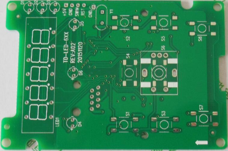
As an important part of electronic products, PCB is used as a substrate material. On the entire printed circuit board, it is mainly responsible for the functions of conduction, insulation and support, PCB performance, quality, processability in manufacturing, cost and processing The level and so on all depend on the basic material. How much do you know about common rigid printed circuit board substrate materials? The editor briefly introduces commonly used printed circuit board substrate materials.
Circuit board material introduction
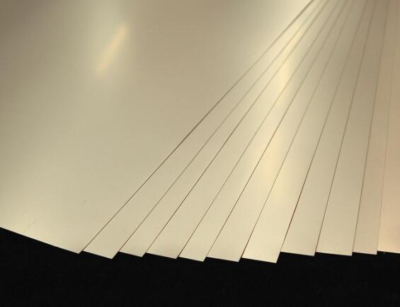
Copper Clad Laminate (Copper Clad Laminate, full name Copper Clad Laminate, CCL in English), is made of wood pulp paper or glass fiber cloth as a reinforcing material, impregnated with resin, covered with copper foil on one or both sides, and then heated and pressed. A finished product, copper clad laminate is also known as substrate, and when it is used in multilayer board production, it is also called core board (CORE).

At present, the copper clad laminates available on the market, considering the base material, can be divided into the following categories: paper substrates, fiberglass cloth substrates, synthetic fiber cloth substrates, non-woven substrates, and composite substrates.
The substrate is an insulating layer board composed of polymer synthetic resin and reinforced materials; the surface of the substrate is covered with a layer of pure copper foil with high conductivity and good solderability, the usual thickness is 35-50/ma; the copper foil is covered on the substrate The copper clad laminate on one side is called single-sided copper clad laminate, and the copper clad laminate with copper foil on both sides of the substrate is called double-sided copper clad laminate; whether the copper foil can be firmly covered on the substrate is completed by the adhesive.
Common materials for circuit boards:
FR-1 ──Phenolic cotton paper, this base material is generally called bakelite (more economical than FR-2)
FR-2 ──Phenolic cotton paper
FR-3 ──Cotton paper, epoxy resin
FR-4──Woven glass, epoxy resin
FR-5 ──Glass cloth, epoxy resin
FR-6 ──Frosted glass, polyester
G-10 ──Glass cloth, epoxy resin
CEM-1 ──Tissue paper, epoxy resin (flame retardant)
CEM-2 ──Tissue paper, epoxy resin (non-flame retardant)
CEM-3 ──Glass cloth, epoxy resin
CEM-4 ──Glass cloth, epoxy resin
CEM-5 ──Glass cloth, polyester
AIN ──Aluminum Nitride
SIC ──Silicon Carbide
There are also many types of copper clad laminates. According to the different insulating materials, it can be divided into paper substrate, glass cloth substrate and synthetic fiberboard; according to the different binder resin, it can be divided into phenolic, epoxy, polyester and polytetrafluoroethylene; it can be divided into general and special types according to the purpose. .
Circuit board jigsaw stamp hole introduction
Generally speaking, the PCB jigsaw can use stamp hole technology or double-sided engraved V-groove segmentation technology. When using stamp holes, pay attention to the overlapping edges should be evenly distributed around each jigsaw to avoid welding The PCB board is deformed due to uneven force.

The position of the stamp hole should be close to the inside of the PCB board to prevent the remaining burrs at the stamp hole after the split board from affecting the customer's entire machine assembly. When using a double-sided V-shaped groove, the depth of the V-shaped groove should be controlled at about 1/3 (the sum of the grooves on both sides), and the groove size is required to be accurate and the depth is uniform.
Specification for making jigsaw stamp hole
1. Stamp hole: It is recommended that 5 to 8 holes of 0.60mm (diameter) be arranged in a row (double rows) as a group.
2. The distance between the double-row board and the board must be at least 1.2mm (conventional 1.6 or 2.0mm).
3. The distance between the edge of the hole and the edge of another hole must be at least 0.25mm to 0.35mm (to ensure sufficient support).
4. It is recommended that the stamp hole be added to the center line of the board frame line or extended to 1/3 of the board, if the board edge is lined, it must be avoided.
5. After adding the stamp hole, the shape of the two sides of the hole must be connected with a straight line or (arc), so that it is convenient to move the knife to determine the position, so as to avoid more knife.