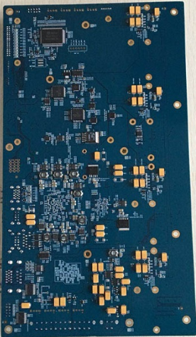
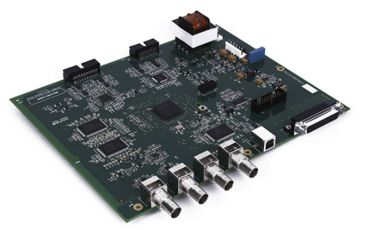
The circuit board tin sinking process is specially designed for the benefit of SMT and chip packaging. The tin metal coating is chemically deposited on the copper surface. It is a new green and environmentally friendly process that replaces the Pb-Sn alloy coating process. It has been widely used in circuits. Among the board surface treatment processes, the following editor will explain in detail what is the circuit board tin sinking process and its characteristics.

Circuit board tin sinking process introduction
Chemical tin sinking is a kind of circuit board tin sinking process, which is widely used. Its working principle is to change the chemical potential of copper ions to cause the stannous ions in the plating bath to undergo a chemical substitution reaction, which is essentially an electrochemical reaction. The reduced tin metal is deposited on the surface of the copper substrate to form a tin plating layer, and the metal complex adsorbed on the immersion tin plating layer catalyzes the reduction of tin ions to metallic tin, so that the tin ions continue to be reduced to tin. The chemical reaction equation is 2Cu+4TU+Sn2-2Cu+(TU)2+Sn.
The thickness of tin sink is about 0.8um-1.2um, the surface structure is loose, the hardness is small, and it is easy to cause surface scratches; sinking tin undergoes a complex chemical reaction with more chemicals, so it is not easy to clean and the surface is easy The residual syrup will cause the problem of discoloration during welding. The storage time is short. It can be stored for three months at normal temperature. If it takes a long time, it will change color.
PCB sinking tin process characteristics
1. Bake at 155 degree Celsius for 4 hours (equivalent to storage for one year), or after 8 days of high temperature and high humidity test (45 degree Celsius, relative humidity 93%), or after three reflow soldering, it still has excellent solderability sex.
2. The tin-immersion layer is smooth, flat and dense, and it is more difficult to form copper-tin intermetallic compounds than tin electroplating, and there is no tin whisker.
3, the thickness of the tin-immersion layer can reach 0.8um-1.2um, which can withstand the impact of lead-free soldering multiple times.
4. The solution is stable, the process is simple, and it can be used continuously through analysis and supplementation without changing the cylinder.
5. Suitable for both vertical and horizontal processes.
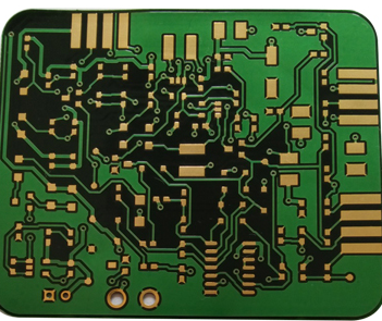
Raw materials needed for circuit board production
1, substrate:
is generally an organic insulating material, and ceramic materials can be used as a substrate for special purposes. Organic insulating materials can be classified into thermosetting resins or thermoplastic polyesters, which are used for rigid or flexible PCBs, respectively. The commonly used thermosetting resins are phenolic resin and epoxy resin, and thermoplastic polyesters are polyimide and polytetrafluoroethylene.
For all PCB substrates, thermosetting resin or thermoplastic polyester (A STAGE) is coated on the base reinforcement material-paper, cloth, glass cloth or glass mat, and then dried in the drying room to remove the resin Or most of the volatile components in the polyester reach a semi-cured state, the so-called B stage, which is also called a prepreg material.

Then select the number of layers of pre-impregnated material according to the thickness of the required substrate, and place the copper foil on the top and bottom according to the single and double panels, and then enter the laminator together-to further solidify the material in a high temperature and high pressure environment, B The stage material is cured into C stage (C STAGE), so the substrate is generally called copper clad laminate. C-stage materials usually have good stability, electrical insulation and chemical resistance.
The substrates made are mainly in 36"*48", 40"*48", and 42"*48" sizes.
2, copper foil:
Most of the metal foils covered on PCBs are copper foils, which are made by calendering or electrolysis. The thickness is generally 0.3mil to 3mil (0.25oz/ft2 to 2oz/ft2), depending on the current carrying current and etching accuracy. The main effects of copper foil on quality are surface dents, pits, and peel strength.
3, PP:
PP is an indispensable interlayer adhesive when preparing multilayer boards, and it is actually a B-stage resin.
4, photosensitive materials:
Photosensitive materials are divided into photoresist and photosensitive film, which are called wet film and dry film in the industry. The coating of the photoresist on the copper clad laminate undergoes chemical changes when exposed to a certain wavelength of light, thereby changing the solubility in the solvent (developer). It also has the difference between positive (photodegradable) and negative (photopolymerizable). Negative resist means that it can be dissolved in the developer before exposure, and the polymer converted after exposure cannot be dissolved. In the developer.
"Positive resist" is the opposite, which generates a polymer that can be dissolved in the developer by sensitization. Photosensitive film, namely dry film, also has negative and positive properties, namely photopolymerization type and photodecomposition type, both of which are very sensitive to ultraviolet rays. There is a big gap between dry film and wet film in price, but because dry film can provide high-precision lines and etching, it has a tendency to replace wet film.
5, solder resist paint:
Solder resist is also called ink. It is actually a kind of solder resist. Commonly, it is a liquid photosensitive material that has no affinity for liquid solder. It will change and harden under specific spectrum irradiation. Others use UV green oil and wet oil, which can be used directly after screen printing. The actual color of the PCB is the color of the solder mask.
6. Negative film:
is also known as film, similar to the polyester film used in photography. It is a material that uses photosensitive material to record image data. It has high contrast, sensitivity and resolution, but requires a low photosensitive speed. The use of glass as the base plate can meet the requirements of fine lines and dimensional stability.