With the high-density interconnection design of PCB circuit boards and the improvement of electronic technology, carbon dioxide (CO2) laser processing equipment has become an important tool for circuit board manufacturers to process PCB circuit board micro-holes, and the development of laser processing PCB micro-hole technology has also improved rapidly. . Let's learn more about it below~
At present, some large-scale printed circuit board manufacturers in the world are gradually adopting carbon dioxide (CO2) laser and UV laser hole forming technology for processing multi-layer PCB multi-layer boards with higher density interconnections, following the continuous development of copper carving crafts technology Improved, carbon dioxide (CO2) laser processing to form holes has been rapidly popularized and widely used in PCB multilayer circuit boards. And further promote the multilayer multilayer board to the field of flip chip packaging, thereby promoting the development of the multilayer multilayer board to a higher density. As a result, the number of blind hole processing holes in multi-layer PCB multilayer boards is increasing, and its single side is generally about 20,000 to 70,000 holes, and even as high as 100,000 holes or more. : For such a large number of blind holes, in addition to using the photo-induced method and plasma method to make the blind holes, especially as the blind via hole diameter becomes smaller and smaller, the use of carbon dioxide (CO2) laser and UV Laser processing to manufacture blind vias is one of the low-cost, high-speed processing methods that circuit board manufacturers can achieve.

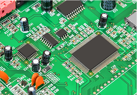
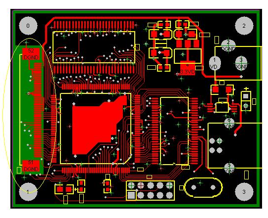
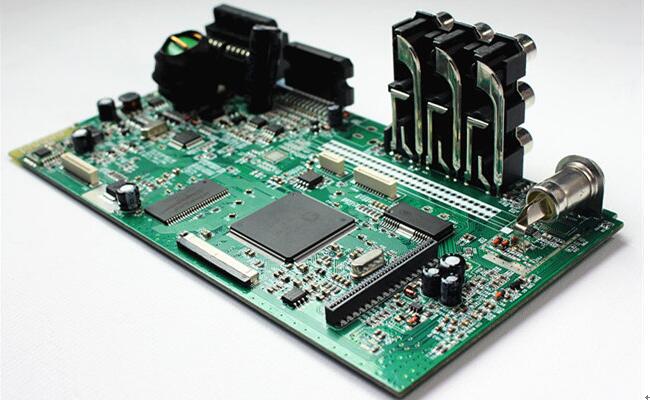
PCB circuit board
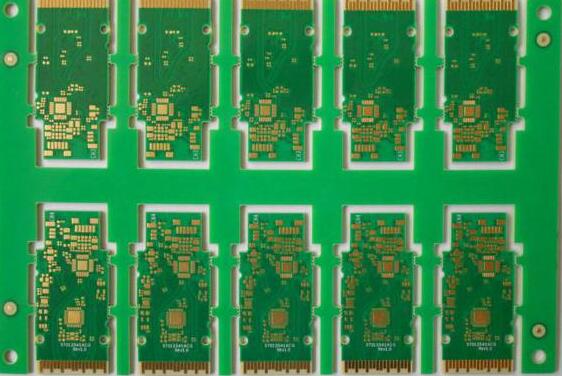
In the late 1980s, AT&T's circuit board R&D department developed carbon dioxide laser processing equipment to process micro-holes on FR-4 PCB circuit boards made of epoxy glass. Because the infrared wavelength of 10.60um is used, the copper skin on the surface of the circuit board cannot be ablated (due to the low infrared absorption rate of metal copper), and the surface of the inner copper (bottom copper) will leave organic carbides on the dielectric The glass fiber cloth (filament) in the layer is not easy to burn or leave a molten state (glass has a low infrared absorption rate), so it must be treated carefully before plating the hole, otherwise it will cause the problem of hole plating or cause the hole wall The roughness is large, so it has not been promoted and applied in the PCB industry. Then IBM and Simens developed gaseous lasers, such as excimer lasers such as argon lasers, krypton lasers, and xenon lasers, with laser wavelengths between 193nm and 308nm (nanomicrons). Although it can effectively avoid the carbonization phenomenon of rabbit organic matter and the problem of glass protrusion melting head, but because of the special inert gas, the processing speed is slow, the output is not messy, and the output (energy) is too low, so it is not in the PCB. The industry has been widely promoted and applied. However, it can be used to effectively remove the carbonized residue caused by the carbon dioxide laser, so the carbon dioxide laser can be used to form a hole, and then the excimer laser can be used to remove the residue to ensure the quality of the laser hole. Double-sided circuit board
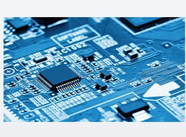
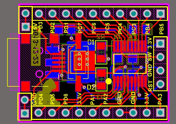
The method of laser processing PCB circuit boards has been applied to circuit board manufacturers so far. Because the micro-hole requirements of multilayer PCB multilayer boards have increased sharply, coupled with the excellence and perfection of CO2 laser equipment and processing technology, CO2 lasers have been rapidly promoted and applied. . At the same time, it has also developed a less chaotic solid-state (bulk) laser device. After multiple harmonics, it can reach the ultraviolet light level laser, because the peak value can reach 12kw, the repetitive power can be at 50, and it is suitable for various kinds of lasers. PCB circuit board materials (including copper foil and glass fiber cloth, etc.), so for the processing of micro-holes less than 0.1 microns, it is undoubtedly one of the most high-density interconnect multi-layer PCB multi-layer boards produced by circuit board manufacturers. Promising processing method. High precision PCB
The laser processing equipment that is actually applied to PCB circuit boards produced by circuit board manufacturers are mainly carbon dioxide lasers and UV lasers. The functions of the laser sources of these two lasers are different. One is for burning copper and the other is It is used for burning the substrate, so the CO2 laser and UV laser are used in the laser processing of PCB circuit boards.